 | –≠–ª–µ–∫—Ç—Ä–æ–Ω–Ω—ã–π –∫–æ–º–ø–æ–Ω–µ–Ω—Ç: AN7918F | –°–∫–∞—á–∞—Ç—å:  PDF PDF  ZIP ZIP |
1
s
Overview
The AN7900T/AN7900F series is 3-pin fixed negative
output type monolithic voltage regulators.
A stabilized fixed negative output voltage is obtained from
an unstable DC input voltage without using any external
parts. Eleven types of fixed output voltage are available
from ≠5V through ≠10V, ≠12V, ≠15V, ≠18V, ≠20V, and
≠24V. They can be used widely as power circuits with a
current capacitance of up to 1A.
s
Features
∑ No external components
∑ Output voltage : ≠5V, ≠6V, ≠7V, ≠8V, ≠9V, ≠10V,
≠12V, ≠15V, ≠18V, ≠20V, ≠24V
∑ Overcurrent limit circuit built-in
∑ Thermal over-load protection built-in
∑ Area of safe operation (ASO) circuit built-in
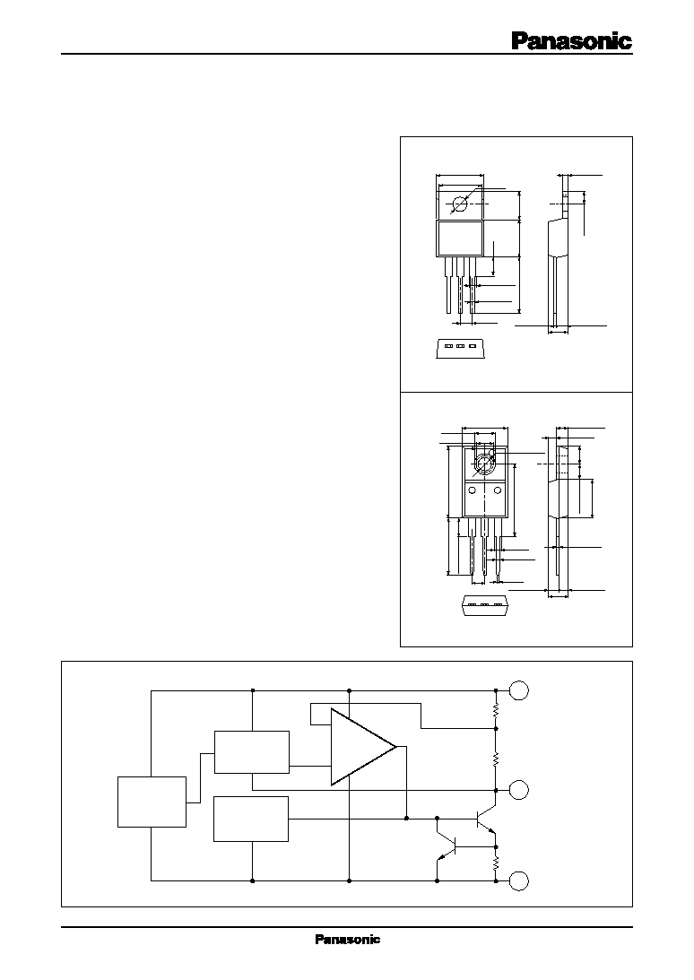
AN7900T/AN7900F Series
3-pin Negative Output Voltage Regulators (1A Type)
s
Block Diagram
1
3
2
Common
Output
Input
Starter
Voltage
Reference
Error Amp.
+
≠
R
1
Q
1
Pass Tr.
R
SC
Current
Limiter
Thermal
Protection
R
2
Unit : mm
AN7900F Series
16.7
±
0.3
17.0
±
0.25
4.2
±
0.25
3.8
±
0.25
8.7
±
0.3
13.6
±
0.25
4.5
±
0.25
1.4
±
0.2
TO-220 Full Pack Package (HSIP003-P-0000A)
10.5
±
0.3
2.77
±
0.3
(1.73)
1
2
3
¯5.3
¯3.1
±
0.1
(4.3)
2.5
±
0.25
4.5
±
0.3
1 : Common
2 : Input
3 : Output
2.0
±
0.25
0.8
±
0.2
(0.4)
2.54
0.4
+ 0. 1
≠ 0.05
Unit : mm
AN7900T Series
10.4
±
0.5
1.4
±
0.1
2.9
±
0.1
6.7
±
0.25
8.7
±
0.3
13.6
±
0.25
1.4
±
0.25
4.5
¯3.7
10.5
±
0.5
2.54
0.45
1 : Common
2 : Input
3 : Output
2.5
±
0.25
+ 0. 1
≠ 0.05
1
2
3
4.5
±
0.3
JEDEC: TO-220AB (HSIP003-P-0000)
0.8
±
0.2
2
V
I
P
D
T
opr
T
stg
V
V
W
∞C
∞C
≠35 *
1
≠40 *
2
15 *
3
10.25 *
3
≠30 to +80
≠55 to +150
Input voltage
Power dissipation
Operating ambient temperature
Storage temperature
AN7900T Series
AN7900F Series
*1 AN7905T/F, AN7906T/F, AN7907T/F, AN7908T/F, AN7909T/F, AN7910T/F, AN7912T/F, AN7915T/F, AN7918T/F
*2 AN7920T/F, AN7924T/F
*3 Follow the derating curve. When T
j
exceeds 150∞C, the internal circuit shuts off the output.
Parameter
Symbol
Rating
Unit
s
Absolute Maximum Ratings
(Ta
=
25∞C)
typ
Output voltage
V
O
≠5.2
V
≠5
Output voltage tolerance
V
O
V
V
I
=
≠7 to ≠20V,
I
O
=
5mA to 1A, P
D
*
Line regulation
REG
IN
100
mV
3
V
I
=
≠7 to ≠25V, T
j
=
25∞C
mV
Load regulation
REG
L
mV
10
I
O
=
5mA to 1.5A, T
j
=
25∞C
mV
I
O
=
250 to 750mA, T
j
=
25∞C
V
I
=
≠8 to ≠12V, T
j
=
25∞C
mA
2
T
j
=
25∞C
1
Bias current
I
bias
mA
V
I
=
≠7 to ≠25V, T
j
=
25∞C
Input bias fluctuation
mA
Load bias current fluctuation
µ
V
40
I
O
=
5mA to 1A, T
j
=
25∞C
Output noise voltage
V
no
dB
f
=
10Hz to 100kHz, Ta
=
25∞C
1.3
0.5
50
≠5.25
100
50
4
62
≠4.8
≠4.75
Ripple rejection ratio
RR
V
I
=
≠8 to ≠18V, I
O
=
100mA, f
=
120Hz
V
1.1
I
O
=
1A, T
j
=
25∞C
Minimum i/o voltage difference
A
2.1
3
74
Peak output current
≠ 0.4
Output voltage temperature coefficient
Parameter
Symbol
Condition
min
max
Unit
T
j
=
25∞C
I
O
=
5mA, T
j
=
0 to 125∞C
T
j
=
25∞C
I
bias (IN)
I
bias (L)
V
DIF (min.)
I
O (Peak)
mV/∞C
V
O
/Ta
Note 1) The specified condition T
j
=
25∞C means that the test should be carried out with the test time so short (within 10ms) that the
drift in characteristic value due to the rise in chip junction temperature can be ignored.
Note 2) Unless otherwise specified, V
I
=
≠10V, I
O
=
500mA, C
I
=
2
µ
F, C
O
=
1
µ
F, T
j
=
0 to 125∞C
* AN7900T series : 15W, AN7900F series : 10.25W
s
Electrical Characteristics
(Ta
=
25∞C)
∑ AN7905T/AN7905F (≠5V Type)
<
=

3
V
O
≠6.25
V
≠6
V
O
V
REG
IN
120
mV
4
mV
REG
L
mV
10
mV
mA
2
1.5
I
bias
mA
mA
44
V
no
dB
1.3
0.5
60
≠6.3
120
60
4
60
≠5.75
≠5.7
RR
V
1.1
A
2.1
3
73
≠ 0.5
typ
Output voltage
Output voltage tolerance
Line regulation
Load regulation
Bias current
Input bias fluctuation
Load bias current fluctuation
Output noise voltage
Ripple rejection ratio
Minimum i/o voltage difference
Peak output current
Output voltage temperature coefficient
Parameter
Symbol
Condition
min
max
Unit
V
I
=
≠8 to ≠21V,
I
O
=
5mA to 1A, P
D
*
V
I
=
≠8 to ≠25V, T
j
=
25∞C
I
O
=
5mA to 1.5A, T
j
=
25∞C
I
O
=
250 to 750mA, T
j
=
25∞C
V
I
=
≠9 to ≠13V, T
j
=
25∞C
T
j
=
25∞C
V
I
=
≠8 to ≠25V, T
j
=
25∞C
µ
V
I
O
=
5mA to 1A, T
j
=
25∞C
f
=
10Hz to 100kHz, Ta
=
25∞C
V
I
=
≠9 to ≠19V, I
O
=
100mA, f
=
120Hz
I
O
=
1A, T
j
=
25∞C
T
j
=
25∞C
I
O
=
5mA, T
j
=
0 to 125∞C
T
j
=
25∞C
I
bias (IN)
I
bias (L)
V
DIF (min.)
I
O (Peak)
mV/∞C
V
O
/Ta
Note 1) The specified condition T
j
=
25∞C means that the test should be carried out with the test time so short (within 10ms) that the
drift in characteristic value due to the rise in chip junction temperature can be ignored.
Note 2) Unless otherwise specified, V
I
=
≠11V, I
O
=
500mA, C
I
=
2
µ
F, C
O
=
1
µ
F, T
j
=
0 to 125∞C
* AN7900T series : 15W, AN7900F series : 10.25W
s
Electrical Characteristics
(Ta
=
25∞C) (continued)
∑ AN7906T/AN7906F (≠6V Type)
<
=
V
O
≠7.3
V
≠7
V
O
V
REG
IN
140
mV
5
mV
REG
L
mV
12
mV
mA
2
1.5
I
bias
mA
mA
48
V
no
dB
1.3
0.5
70
≠7.35
140
70
4
58
≠6.7
≠6.65
RR
V
1.1
A
2.1
4
72
≠ 0.5
typ
Output voltage
Output voltage tolerance
Line regulation
Load regulation
Bias current
Input bias fluctuation
Load bias current fluctuation
Output noise voltage
Ripple rejection ratio
Minimum input/output voltage difference
Peak output current
Output voltage temperature coefficient
Parameter
Symbol
Condition
min
max
Unit
V
I
=
≠79 to ≠22V,
I
O
=
5mA to 1A, P
D
*
V
I
=
≠9 to ≠25V, T
j
=
25∞C
I
O
=
5mA to 1.5A, T
j
=
25∞C
I
O
=
250 to 750mA, T
j
=
25∞C
V
I
=
≠10 to ≠14V, T
j
=
25∞C
T
j
=
25∞C
V
I
=
≠9 to ≠25V, T
j
=
25∞C
µ
V
I
O
=
5mA to 1A, T
j
=
25∞C
f
=
10Hz to 100kHz, Ta
=
25∞C
V
I
=
≠10 to ≠20V, I
O
=
100mA, f
=
120Hz
I
O
=
1A, T
j
=
25∞C
T
j
=
25∞C
I
O
=
5mA, T
j
=
0 to 125∞C
T
j
=
25∞C
I
bias (IN)
I
bias (L)
V
DIF (min.)
I
O (Peak)
mV/∞C
V
O
/Ta
Note 1) The specified condition T
j
=
25∞C means that the test should be carried out with the test time so short (within 10ms) that the
drift in characteristic value due to the rise in chip junction temperature can be ignored.
Note 2) Unless otherwise specified, V
I
=
≠12V, I
O
=
500mA, C
I
=
2
µ
F, C
O
=
1
µ
F, T
j
=
0 to 125∞C
* AN7900T series : 15W, AN7900F series : 10.25W
∑ AN7907T/AN7907F (≠7V Type)
<
=
4
V
O
≠8.3
V
≠8
V
O
V
REG
IN
160
mV
6
mV
REG
L
mV
12
mV
mA
2.2
2
I
bias
mA
mA
52
V
no
dB
1
0.5
80
≠8.4
160
80
4.5
56
≠7.7
≠7.6
RR
V
1.1
A
2.1
4
71
≠ 0.6
typ
Output voltage
Output voltage tolerance
Line regulation
Load regulation
Bias current
Input bias fluctuation
Load bias current fluctuation
Output noise voltage
Ripple rejection ratio
Minimum input/output voltage difference
Peak output current
Output voltage temperature coefficient
Parameter
Symbol
Condition
min
max
Unit
V
I
=
≠10 to ≠23V,
I
O
=
5mA to 1A, P
D
*
V
I
=
≠10.5 to ≠25V, T
j
=
25∞C
I
O
=
5mA to 1.5A, T
j
=
25∞C
I
O
=
250 to 750mA, T
j
=
25∞C
V
I
=
≠11 to ≠17V, T
j
=
25∞C
T
j
=
25∞C
V
I
=
≠10.5 to ≠25V, T
j
=
25∞C
µ
V
I
O
=
5mA to 1A, T
j
=
25∞C
f
=
10Hz to 100kHz, Ta
=
25∞C
V
I
=
≠11 to ≠21V, I
O
=
100mA, f
=
120Hz
I
O
=
1A, T
j
=
25∞C
T
j
=
25∞C
I
O
=
5mA, T
j
=
0 to 125∞C
T
j
=
25∞C
I
bias (IN)
I
bias (L)
V
DIF (min.)
I
O (Peak)
mV/∞C
V
O
/Ta
Note 1) The specified condition T
j
=
25∞C means that the test should be carried out with the test time so short (within 10ms) that the
drift in characteristic value due to the rise in chip junction temperature can be ignored.
Note 2) Unless otherwise specified, V
I
=
≠14V, I
O
=
500mA, C
I
=
2
µ
F, C
O
=
1
µ
F, T
j
=
0 to 125∞C
* AN7900T series : 15W, AN7900F series : 10.25W
s
Electrical Characteristics
(Ta
=
25∞C) (continued)
∑ AN7908T/AN7908F (≠8V Type)
<
=
V
O
≠9.35
V
≠9
V
O
V
REG
IN
180
mV
7
mV
REG
L
mV
12
mV
mA
2.2
2
I
bias
mA
mA
58
dB
1
0.5
90
≠9.45
180
90
4.5
56
≠8.65
≠8.55
RR
V
1.1
A
2.1
4
71
≠0.6
typ
Output voltage tolerance
Input bias fluctuation
Load bias current fluctuation
Output noise voltage
Ripple rejection ratio
Minimum input/output voltage difference
Peak output current
Output voltage temperature coefficient
Parameter
Symbol
Condition
min
max
Unit
Output voltage
Line regulation
Load regulation
Bias current
V
no
V
I
=
≠11.5 to ≠24V,
I
O
=
5mA to 1A, P
D
*
V
I
=
≠11.5 to ≠26V, T
j
=
25∞C
I
O
=
5mA to 1.5A, T
j
=
25∞C
I
O
=
250 to 750mA, T
j
=
25∞C
V
I
=
≠12 to ≠18V, T
j
=
25∞C
T
j
=
25∞C
V
I
=
≠11.5 to ≠26V, T
j
=
25∞C
µ
V
I
O
=
5mA to 1A, T
j
=
25∞C
f
=
10Hz to 100kHz, Ta
=
25∞C
V
I
=
≠12 to ≠22V, I
O
=
100mA, f
=
120Hz
I
O
=
1A, T
j
=
25∞C
T
j
=
25∞C
I
O
=
5mA, T
j
=
0 to 125∞C
T
j
=
25∞C
I
bias (IN)
I
bias (L)
V
DIF (min.)
I
O (Peak)
mV/∞C
V
O
/Ta
Note 1) The specified condition T
j
=
25∞C means that the test should be carried out with the test time so short (within 10ms) that the
drift in characteristic value due to the rise in chip junction temperature can be ignored.
Note 2) Unless otherwise specified, V
I
=
≠15V, I
O
=
500mA, C
I
=
2
µ
F, C
O
=
1
µ
F, T
j
=
0 to 125∞C
* AN7900T series : 15W, AN7900F series : 10.25W
∑ AN7909T/AN7909F (≠9V Type)
<
=
5
V
O
≠10.4
V
≠10
V
O
V
REG
IN
200
mV
8
mV
REG
L
mV
12
mV
mA
2.5
2.5
I
bias
mA
mA
64
V
no
dB
1
0.5
100
≠10.5
200
100
5
56
≠9.6
≠9.5
RR
V
1.1
A
2.1
4
71
≠ 0.7
typ
Output voltage
Output voltage tolerance
Line regulation
Load regulation
Bias current
Input bias fluctuation
Load bias current fluctuation
Output noise voltage
Ripple rejection ratio
Minimum input/output voltage difference
Peak output current
Output voltage temperature coefficient
Parameter
Symbol
Condition
min
max
Unit
V
I
=
≠12.5 to ≠25V,
I
O
=
5mA to 1A, P
D
*
V
I
=
≠12.5 to ≠27V, T
j
=
25∞C
I
O
=
5mA to 1.5A, T
j
=
25∞C
I
O
=
250 to 750mA, T
j
=
25∞C
V
I
=
≠13 to ≠19V, T
j
=
25∞C
T
j
=
25∞C
V
I
=
≠12.5 to ≠27V, T
j
=
25∞C
µ
V
I
O
=
5mA to 1A, T
j
=
25∞C
f
=
10Hz to 100kHz, Ta
=
25∞C
V
I
=
≠13 to ≠23V, I
O
=
100mA, f
=
120Hz
I
O
=
1A, T
j
=
25∞C
T
j
=
25∞C
I
O
=
5mA, T
j
=
0 to 125∞C
T
j
=
25∞C
I
bias (IN)
I
bias (L)
V
DIF (min.)
I
O (Peak)
mV/∞C
V
O
/Ta
Note 1) The specified condition T
j
=
25∞C means that the test should be carried out with the test time so short (within 10ms) that the
drift in characteristic value due to the rise in chip junction temperature can be ignored.
Note 2) Unless otherwise specified, V
I
=
≠16V, I
O
=
500mA, C
I
=
2
µ
F, C
O
=
1
µ
F, T
j
=
0 to 125∞C
* AN7900T series : 15W, AN7900F series : 10.25W
s
Electrical Characteristics
(Ta
=
25∞C) (continued)
∑ AN7910T/AN7910F (≠10V Type)
<
=
V
O
≠12.5
V
≠12
V
O
V
REG
IN
240
mV
10
mV
REG
L
mV
12
mV
mA
2.5
3
I
bias
mA
mA
75
V
no
dB
1
0.5
120
≠12.6
240
120
5
55
≠11.5
≠11.4
RR
V
1.1
A
2.1
4
70
≠ 0.8
typ
Output voltage
Output voltage tolerance
Line regulation
Load regulation
Bias current
Input bias fluctuation
Load bias current fluctuation
Output noise voltage
Ripple rejection ratio
Minimum input/output voltage difference
Peak output current
Output voltage temperature coefficient
Parameter
Symbol
Condition
min
max
Unit
V
I
=
≠14.5 to ≠27V,
I
O
=
5mA to 1A, P
D
*
V
I
=
≠14.5 to ≠30V, T
j
=
25∞C
I
O
=
5mA to 1.5A, T
j
=
25∞C
I
O
=
250 to 750mA, T
j
=
25∞C
V
I
=
≠16 to ≠22V, T
j
=
25∞C
T
j
=
25∞C
V
I
=
≠14.5 to ≠30V, T
j
=
25∞C
µ
V
I
O
=
5mA to 1A, T
j
=
25∞C
f
=
10Hz to 100kHz, Ta
=
25∞C
V
I
=
≠15 to ≠25V, I
O
=
100mA, f
=
120Hz
I
O
=
1A, T
j
=
25∞C
T
j
=
25∞C
I
O
=
5mA, T
j
=
0 to 125∞C
T
j
=
25∞C
I
bias (IN)
I
bias (L)
V
DIF (min.)
I
O (Peak)
mV/∞C
V
O
/Ta
Note 1) The specified condition T
j
=
25∞C means that the test should be carried out with the test time so short (within 10ms) that the
drift in characteristic value due to the rise in chip junction temperature can be ignored.
Note 2) Unless otherwise specified, V
I
=
≠19V, I
O
=
500mA, C
I
=
2
µ
F, C
O
=
1
µ
F, T
j
=
0 to 125∞C
* AN7900T series : 15W, AN7900F series : 10.25W
∑ AN7912T/AN7912F (≠12V Type)
<
=