 | –≠–ª–µ–∫—Ç—Ä–æ–Ω–Ω—ã–π –∫–æ–º–ø–æ–Ω–µ–Ω—Ç: AN9DB00 | –°–∫–∞—á–∞—Ç—å:  PDF PDF  ZIP ZIP |
Analog Master Slice
1
AN9D, AN9E, AN9F Series
Analog master slice IC series
s
Overview
The AN9D, AN9E and AN9F series are master slice ICs of bipolar process, which enables you to integrate an analog
circuit easily onto a single chip. A custom IC can be made by placing a wired pattern designed in line with the customer's
analog circuit onto a master slice.
Starting from a wafer on which a most part of IC diffusion processes are already finished, you can shorten an IC pilot
fabrication considerably. Further, placement of elements and inter-element wiring are done automatically by a com-
puter, which results in short period of pattern designing and thereby developing a custom IC in a short period.
s
Features
∑
High design flexibility
∑ Easy circuit constant design because of setting resistance or capacitance to an arbitrary value.
∑ Free setting of contacts between a substrate and GND wiring prevents from operation error to be caused by floating
of substrate potential.
∑ Usable for multi power source because a resistor island potential can be set for each unit.
∑ Builds in a lateral type PNP transistor of high reverse breakdown voltage between base and emitter, or a collector
wall type NPN transistor of excellent saturation characteristics. (AN9DA00, AN9DB00, AN9DF00)
∑
Short development period
∑ Due to a full automatic layout design, a sample is available in one month from a completion of a circuit diagram.
∑
Applicable to a small quantity production item
∑ Possible to develop a custom IC for small quantity production due to a low development cost.
s
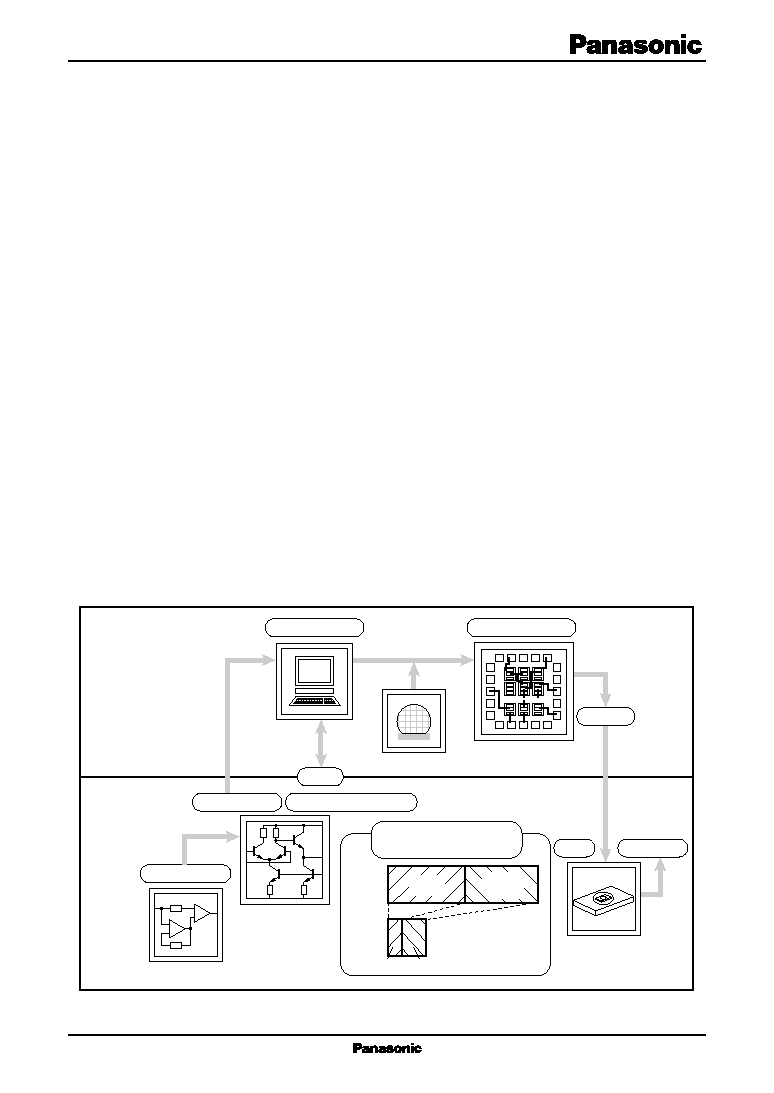
Development Flow
1 000 elements in case
of general-use process
1week 3weeks
Full
custom
Master
slice
Layout
8weeks
Diffusion,
assembly
6weeks
EWS
Matsushita side
Customer side
Full automatic
layout
Mask layout
System design
Circuit design
Test specification, etc.
Drastic shrinkage of TAT
for small quantity production
Wiring, assembly
Fabricated wafer
Check
Chip
Evaluation
Wired mask only
Selection
AN9D, AN9E, AN9F Series
Analog Master Slice
2
s
Product Mix
Element characteristics
Series name
Supply
NPN transistor
PNP transistor
Remarks
voltage
f
T(max)
BV
CEO
h
FE
f
T(max)
BV
CEO
h
FE
AN9D series to 12 V
2.6 GHz
14.4 V 100 to 250 1.0 GHz
14.4 V
66 to 200
For low power dissipation/
high speed operation IC
AN9E series
to 12 V 3.5 GHz
14.4 V
80 to 250 1.5 GHz
14.4 V
50 to 130
For Bi-CMOS IC
AN9F series
to 30 V 300 MHz
30 V
80 to 250
9 MHz
30 V
80 to 350
For high breakdown
voltage IC
s
Basic Block Configuration (AN9DA00, AN9DB00, AN9DF00)
SP2 resistor
(variable)
SP2 resistor
(variable)
SP resistor
(fixed)
SP resistor
(fixed)
Capacitance
PNP transistor
(lateral type)
PNP transistor
(vertical type)
NPN transistor
(collector wall type)

Analog Master Slice
AN9D, AN9E, AN9F Series
3
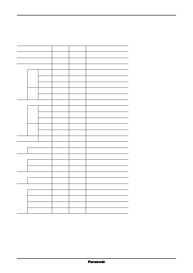
Product name
AN9DA00 AN9DB00 AN9DC00 AN9DE00 AN9DD00
*
AN9DF00
Remarks
Pad count
28
36
55
64
75
32
Total element count
1 287
2 424
3 854
5 106
6 602
1 607
Transistor count
306
600
920
1 288
1 610
306
A11
320
448
560
Basic size
NPN
A21
160
224
280
Double size
A62P
8
8
8
62 times size
B11
126
252
126
Basic size (CW winding)
LA1
84
168
84
Basic size (Lateral type)
PNP
LA4S
4
4
4
8 times size (Lateral type)
V11
84
168
320
448
560
84
Basic size (Vertical type)
V21
120
168
210
Double size (Vertical type)
Gate countIIL
320
Resistor count
969
1 800
2 854
3 706
4 852
969
SP
5 k
474
888
1 408
1 728
2 440
474
10 k
198
336
480
640
800
198
SP2
2.5 k
297
576
966
1 338
1 612
297
Resistance variable
Capacitor count 5 pF
12
24
80
112
140
12
Note) *: Under development
∑
AN9D series (V
CC
=
to 12 V, f
T(max)
=
2.6 GHz)
∑ High speed low power dissipation process
∑ Constant-variable resistor and capacitor elements built in
∑ Large current transistor built in (AN9DA00, AN9DB00, AN9DF00)
∑ Optimal for a control-system application due to built-in collector wall type NPN transistors and lateral PNP transis-
tors (AN9DA00, AN9DB00, AN9DF00)
∑ Optimal for signal processing application due to built-in high speed NPN transistors and vertical PNP transistors
(AN9DC00, AN9DD00, AN9DE00)
∑ IIL element built-in (AN9DF00)
AN9D, AN9E, AN9F Series
Analog Master Slice
4
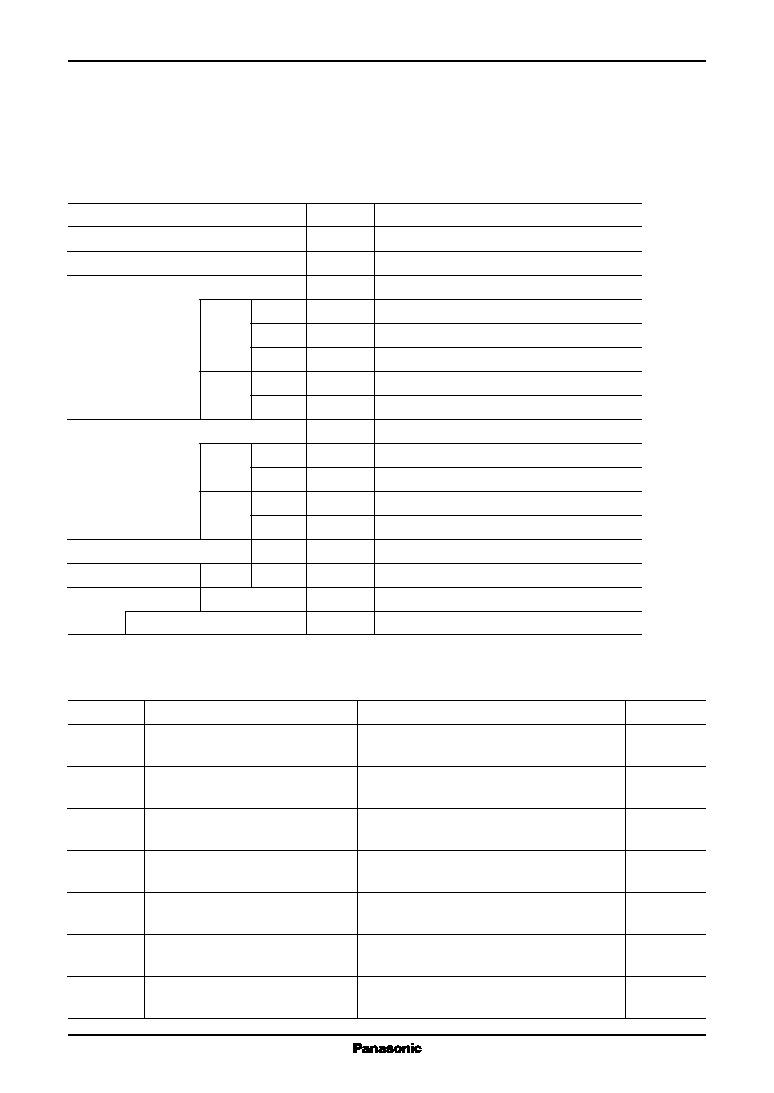
Product name
AN9EA00
*
AN9EB00
*
Remarks
Pad count
40
55
Total element count
8 830
14 033
Transistor count
900
1 402
N21
420
588
Double size
NPN
N54
20
34
40 times size
A42G
20
96
PNP
P21
420
588
Double size (Vertical type)
V42G
20
96
Resistor count
5 016
7 138
40 k
90
160
SP
10 k
1 440
2 016
5 k
1 680
2 352
PS
5 k
1 086
1 602
Resistance variable
2 k
720
1 008
Resistance variable
Capacitor count
5 pF
60
84
Diode count
30
42
ZD1
30
42
Zener zap element
MOS count
12
32
N-MOS
6
16
60/2
P-MOS
6
16
30/2
Gate array count
2 800
5 400
LOGIC
2 800
5 400
Use rate 35% or less
Standard cell count
12
19
Analog SW
6
12
Analog SW
4
4
8-bit DAC
1
1
Oscillation circuit
1
2
Note) *: Under development
∑
AN9E series (V
CC
=
to 12 V, f
T(max)
=
3.5 GHz)
∑ Bi-CMOS process adopted
∑ Constant-variable resistor and capacitor elements built in
∑ Gate array and standard cell built in
∑ Zener zap elements built in
Analog Master Slice
AN9D, AN9E, AN9F Series
5
Product name
AN9FA00
Remarks
Pad count
36
Total element count
1 655
Transistor count
308
N11X
72
Basic size
NPN
W11X
72
Basic size (surrounded with DN)
N100X
8
100 times size
PNP
YA1
144
Basic size (Lateral type)
YX1DP
12
Emitter and collector are surrounded with DN
Resistor count
1 308
SP
2 k
1 068
Resistance variable
5 k
48
Resistance variable
PW
10 k
136
50 k
56
Capacitor count
7.5 pF
24
Capacitance variable
Diode count
ZD
ZB2
15
Bulk Zener diode
Special block
Output circuit
3
250 times size transistor built-in
Reference power supply circuit
1
2.5 V reference power supply circuit
Circuit name
Contents
Features
Remarks
Op-amp.1
General-use
Wide output D-range: 0.2 V to V
CC
-
0.5 V
AN9D series
Single power supply operational amp.
Low power consumption: I
CC
=
0.5 mA
Op-amp.2
High speed
High speed: Cutoff frequency
=
20 MHz
AN9D series
Highly stable operational amp.
: Slew rate
=
100 V/
µ
s
Op-amp.3
General-use
Low power consumption: I
CC
=
0.15 mA
AN9D series
Single power supply operational amp.
Op-amp.4
General-use
High gain: Voltage gain
=
107 dB
AN9D series
Single power supply operational amp.
High stability: Phase margin
=
43
∞
Comp1
Low power consumption
Low power consumption: I
CC
=
0.1 mA
AN9D series
Single power supply comparator
High speed: t
r
/
t
f
=
0.15
µ
s/0.3
µ
s
Comp2
Single power supply
High speed: t
d
=
0.015
µ
s
AN9D series
High speed comparator
Reg1
General-use
High temp. stability: 150 ppm/degree or less
AN9D series
Stabilized power supply
Wide output voltage range: 1.3 V to V
CC
-
0.5 V
s
Circuit Library
General-use basic circuits are available as libraries.
∑
AN9F series (V
CC
=
to 30 V, f
T(max)
=
300 MHz)
∑ High voltage process adopted
∑ Constant-variable resistor and capacitor elements built in
∑ Built-in Zener diode for simplified reference voltage
∑ Output-circuit-exclusive three blocks are built in
∑ ZAP-adopted reference-voltage-exclusive one block is built in

AN9D, AN9E, AN9F Series
Analog Master Slice
6
s
Package Table
Series name
AN9DX00 series
AN9EX00 series AN9FX00
Master name
AN9DA00 AN9DB00 AN9DC00 AN9DD00 AN9DE00 AN9DF00 AN9EA00 AN9EB00 AN9FA00
Package Pin count
16
q
18
DIL
20
22
q
q
q
24
q
28
q
q
q
20
q
q
22
q
q
24
q
q
q
SDIL
28
q
q
q
q
q
q
30
q
q
q
42
q
q
q
52
q
q
q
q
18
20
q
q
q
SO
22
24
q
q
28
q
q
q
q
q
q
q
q
36
q
q
q
q
32
q
q
44
q
QPF
48
q
q
q
64
q
q
q
q
q
q
80
q
q
QFN
24
q
44
q
q
q
q
q
q
q