1
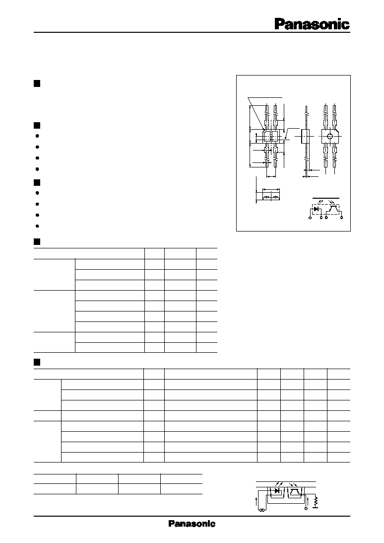
Reflective Photosensors (Photo Reflectors)
*1
Input power derating ratio is
1.0 mW/∞C at Ta
25∞C.
*2
Output power derating ratio is
0.67 mW/∞C at Ta
25∞C.
2.0
±
0.2
2.0
±
0.2
Mark for indicating
emitter side
C0.5
3.4
±
0.3
0.4
2.7
±
0.2
9.0
±
1.0
9.0
±
1.0
Chip
center
1.8
2
4
1
3
4-0.5
±
0.1
4-0.7
0.5
0.15
Pin connection
Unit : mm
1.5
±
0.2
3
2
1
4
,,
,
,
,,
V
CC
R
L
I
F
I
C
,,
,,,
,,,
,,,
,,,
,,
Evaporated Al
Glass plate
(t = 1mm)
Absolute Maximum Ratings
(Ta = 25∞C)
Parameter
Symbol Ratings
Unit
Input (Light
Reverse voltage (DC)
V
R
3
V
emitting diode)
Forward current (DC)
I
F
50
mA
Power dissipation
P
D
*1
75
mW
Collector current
I
C
20
mA
Output (Photo Collector to emitter voltage
V
CEO
30
V
transistor)
Emitter to collector voltage
V
ECO
5
V
Collector power dissipation
P
C
*2
50
mW
Temperature
Operating ambient temperature
T
opr
≠25 to +85
∞C
Storage temperature
T
stg
≠30 to +100
∞C
Electrical Characteristics
(Ta = 25∞C)
Parameter
Symbol
Conditions
min
typ
max
Unit
Input
Forward voltage (DC)
V
F
I
F
= 50mA
1.3
1.5
V
characteristics
Reverse current (DC)
I
R
V
R
= 3V
0.01
10
µ
A
Capacitance between terminals
C
t
V
R
= 0V, f
= 1MHz
30
pF
Output characteristics Collector cutoff current
I
CEO
V
CE
= 10V
200
nA
Collector current
I
C
*1, *2
V
CC
= 5V, I
F
= 10mA, R
L
= 100
, d
= 1mm
90
880
µ
A
Transfer
Leakage current
I
D
V
CC
= 5V, I
F
= 10mA, R
L
= 100
200
nA
characteristics Response time
t
r
*3
, t
f
*4
V
CC
= 5V, I
C
= 0.1mA, R
L
= 100
20
µ
s
Collector to emitter saturation voltage V
CE(sat)
I
F
= 20mA, I
C
= 0.1mA
0.4
V
Features
Ultraminiature, thin type : 2.7
◊
3.4 mm (height : 1.5 mm)
Visible light cutoff resin is used
Fast response : t
r
, t
f
= 20
µ
s (typ.)
Easy interface for control circuit
Applications
Control of motor and other rotary units
Detection of position and edge
Detection of paper, film and cloth
Start, end mark detection of magnetic tape
CNB1303
Reflective Photosensor
Overview
CNB1303 is a small, thin reflective photosensor consisting of a
high efficiency GaAs infrared light emitting diode which is integrated
with a high sensitivity Si phototransistor in a single resin package.
*2
Output current measurement method
*3
Time required for the output current to increase from 10% to 90% of its final value
*4
Time required for the output current to decrease from 90% to 10% of its initial value
*1
I
C
classifications
Class
Q
R
S
I
C
(
µ
A)
90 to 220
180 to 440
360 to 880
2
CNB1303
Reflective Photosensors (Photo Reflectors)
I
F
, I
C
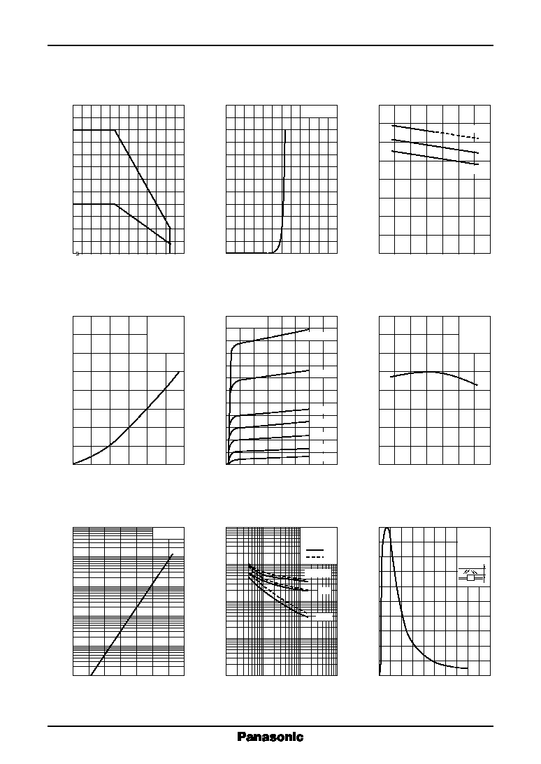
-- Ta
Forward current, collector current I
F
, I
C
(mA)
60
50
40
30
20
10
Ambient temperature Ta (∞C )
0
20
40
60
80
100
0
≠ 25
I
F
I
C
I
F
-- V
F
60
30
20
10
50
40
Forward voltage V
F
(V)
Forward current I
F
(mA)
0.4
0.8
1.2
1.6
2.4
2.0
0
0
Ta = 25∞C
V
F
-- Ta
1.6
1.2
0.8
0.4
Ambient temperature Ta (∞C )
Forward voltage V
F
(V)
0
20
40
60
80
100
0
≠ 40 ≠ 20
0
20
40
60
80
100
≠ 40 ≠ 20
0
20
40
60
80
100
≠ 40 ≠ 20
I
C
-- I
F
Forward current I
F
(mA)
Collector current I
C
(
µ
A)
800
400
200
600
8
16
24
0
0
V
CC
= 5V
Ta = 25∞C
R
L
= 100
d = 1mm
Relative output current I
C
(%)
I
C
-- Ta
160
120
80
40
Ambient temperature Ta (∞C )
0
V
CC
= 5V
I
F
= 10mA
R
L
= 100
I
CEO
-- Ta
10
10
≠2
1
10
≠3
10
≠1
Ambient temperature Ta (∞C )
V
CE
= 10V
Dark current I
CEO
(
µ
A)
10
≠4
1
10
10
≠1
t
r
, t
f
-- I
C
1
Collector current I
C
(mA)
Rise time , fall time t
r
, t
f
(
µ
s)
10
≠1
10
≠2
10
3
10
2
10
V
CC
= 5V
Ta = 25∞C
: t
r
: t
f
Distance d (mm)
I
C
-- d
100
60
40
20
80
Relative output current I
C
(%)
2
4
6
10
8
0
0
V
CC
= 5V
Ta = 25∞C
I
F
= 10mA
I
C
-- V
CE
Collector to emitter voltage V
CE
(V)
Collector current I
C
(mA)
600
400
300
200
100
500
4
6
8
0
0
d = 1mm
Ta = 25∞C
2
15mA
10mA
8mA
6mA
4mA
2mA
I
F
= 20mA
R
L
= 2k
1k
100
d
,
,,
10mA
1mA
I
F
= 50mA