
1
Optoisolators (Photocouplers)
CNC1S101, CNZ3132, CNZ3133, CNZ3134
(ON3131, ON3132, ON3133, ON3134)
Optoisolators
Overview
CNC1S101 is a DIL type 4-pin single-channel optoisolator which is
housed in a small package. This optoisolator series also includes the two-
channel CNZ3132, the three-channel CNZ3133, and the four-channel 3134.
The CNC1S101 series has a number of good features, including high I/O
isolation voltage and current transfer ratio (CTR), as well as high speed
response.
Features
High current transfer ratio : CTR
100%
High I/O isolation voltage : V
ISO
= 5000 V
rms
(min.)
Fast response : t
r
= 2
µ
s, t
f
= 3
µ
s (typ.)
Low dark current : I
CEO
100 nA
UL listed (UL File No. E79920)
Applications
Switching power supply
Computer terminal equipment
System equipment, measuring equipment
Telephones, copier, vending machines
Televisions, VCRs, and other consumer electronics products
Medical equipment and phsical and chemical equipment
Signal transmission between circuits with different potentials
and impedances
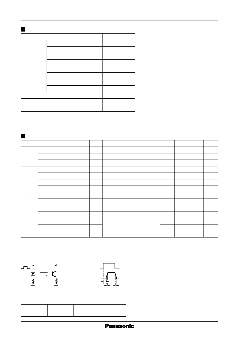
Unit : mm
CNC1S101
CNZ3132
CNZ3133
CNZ3134
Unit : mm
Unit : mm
Unit : mm
1: Anode
2: Cathode
3: Emitter
4: Collector
1,3: Anode
2,4: Cathode
5,7: Emitter
6,8: Collector
1,3,5: Anode
2,4,6: Cathode
7,9,11: Emitter
8,10,12: Collector
1,3,5,7: Anode
2,4,6,8: Cathode
9,11,13,15: Emitter
10,12,14,16: Collector
0 to 15∞
0 to 15∞
0 to 15∞
0 to 15∞
1
2
3
4
4.58
±
0.3
1
2
3
4
6
5
8
7
9.66
±
0.3
0.25
4-0.5
±
0.1
4-1.2
±
0.15
2.54
±
0.25
2.0
3.85
±
0.3
+0.15 ≠0
7.62
±
0.3
2.54 min.
0.5 min.
6.2
±
0.5
0.25
2.0
3.85
±
0.3
+0.15 ≠0
7.62
±
0.3
6.2
±
0.5
0 to 15∞
0 to 15∞
1
2
3
4
5
6
9
10
11
12
7
8
14.74
±
0.3
1
2
3
4
5
6
7
8
13
14
15
16
9
10
11
12
19.82
±
0.5
0.25
2.0
3.85
±
0.3
+0.15 ≠0
7.62
±
0.3
6.2
±
0.5
0 to 15∞
0 to 15∞
0.25
2.0
3.85
±
0.3
+0.15 ≠0
7.62
±
0.3
6.2
±
0.5
5.2 max.
8-0.5
±
0.1
8-1.2
±
0.15
2.54
±
0.25
2.54 min.
0.5 min.
5.2 max.
12-0.5
±
0.1
12-1.2
±
0.15
2.54
±
0.25
2.54 min.
0.5 min.
5.2 max.
16-0.5
±
0.1
16-1.2
±
0.15
2.54
±
0.25
2.54 min.
0.5 min.
5.2 max.
LED Mark
LED Mark
LED Mark
LED Mark
Pin Connection
Top View
Top View
CNC1S101
Top View
CNZ3133
1
2
4
3
1
2
12
11
3
4
10
9
5
6
8
7
1
2
8
7
3
4
6
5
1
2
16
15
3
4
14
13
5
6
12
11
7
8
10
9
CNZ3132
Top View
CNZ3134
Note) The part numbers in the parenthesis show conventional part number.
2
CNC1S101,CNZ3132,CNZ3133,CNZ3134
Optoisolators (Photocouplers)
;;
;
;
(Input pulse)
(Output pulse)
50
R
L
t
d
: Delay time
V
CC
Sig.OUT10%
90%
Sig.IN
t
d
t
r
t
f
Absolute Maximum Ratings
(Ta = 25∞C)
Parameter
Symbol Ratings
Unit
Reverse voltage (DC)
V
R
6
V
Input (Light
Forward current (DC)
I
F
50
mA
emitting diode)
Pulse forward current
I
FP
*1
1
A
Power dissipation
P
D
*2
75
mW
Collector current
I
C
50
mA
Output (Photo Collector to emitter voltage
V
CEO
80
V
transistor)
Emitter to collector voltage
V
ECO
7
V
Collector power dissipation
P
C
*3
150
mW
Total power dissipation
P
T
200
mW
Operating ambient temperature
T
opr
≠30 to +100
∞C
Storage temperature
T
stg
≠55 to +125
∞C
*1
Pulse width
100
µ
s, repeat 100 pps
*2
Input power derating ratio is 0.75 mW/∞C at Ta
25∞C.
*3
Output power derating ratio is 1.5 mW/∞C at Ta
25∞C.
Electrical Characteristics
(Ta = 25∞C)
Parameter
Symbol
Conditions
min
typ
max
Unit
Input
Reverse current (DC)
I
R
V
R
= 3V
10
µ
A
characteristics
Forward voltage (DC)
V
F
I
F
= 50mA
1.35
1.5
V
Capacitance between pins
C
t
V
R
= 0V, f
= 1MHz
15
pF
Collector cutoff current
I
CEO
V
CE
= 20V
5
100
nA
Output
Collector to emitter voltage
V
CEO
I
C
= 100
µ
A
80
V
characteristics Collector to emitter capacitance
C
C
V
CE
= 10V, f
= 1MHz
3
pF
Emitter to collector voltage
V
ECO
I
E
= 10
µ
A
7
V
DC current transfer ratio
CTR
*1, *5
V
CE
= 5V, I
F
=5mA
100
600
%
Isolation voltage, input to output
V
ISO
t
= 1 min., RH < 60%
5000
V
rms
Isolation capacitance, input to output
C
ISO
f
= 1MHz
0.7
pF
Transfer
Isolation resistance, input to output
R
ISO
V
ISO
= 500V
10
11
characteristics
Rise time
t
r
*2, *4
V
CC
= 10V, I
C
= 2mA
2
µ
s
Fall time
t
f
*3,
*4
R
L
= 100
3
µ
s
Collector to emitter saturation voltage V
CE(sat)
I
F
= 20mA, I
C
= 1mA
0.1
0.2
V
*1
DC current transfer ratio (CTR) is a ratio of output current against DC input current.
*2
t
r
: Time required for the collector current to increase from 10% to 90% of its final value
*3
t
f
: Time required for the collector current to decrease from 90% to 10% of its initial value
*4
Rise and fall time measurement circuit
*5
CTR classifications
Class
General
R
S
CTR (%)
100 to 600
100 to 300
200 to 600
3
Optoisolators (Photocouplers)
CNC1S101,CNZ3132,CNZ3133,CNZ3134
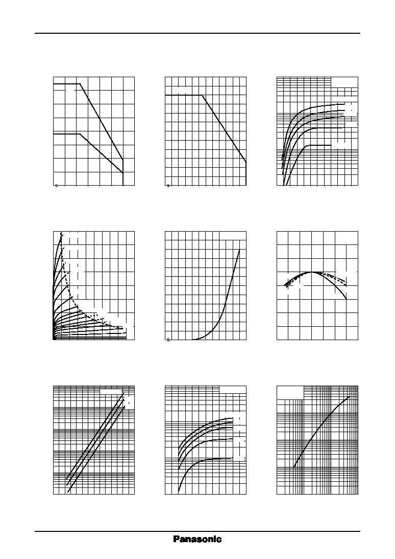
I
F
, I
C
-- Ta
Forward current, collector current I
F
, I
C
(mA)
I
C
-- V
CE
Collector to emitter voltage V
CE
(V)
Collector current I
C
(mA)
Ta = 25∞C
10
2
1
10
0
0.2
0.4
0.6
0.1
0.3
0.5
10
≠1
I
C
-- V
CE
40
10
20
30
Collector to emitter voltage V
CE
(V)
Collector current I
C
(mA)
8
16
24
40
32
0
0
60
50
40
30
20
10
Ambient temperature Ta (∞C )
0
20
40
60
80
100
0
≠ 30
P
C
, P
D
-- Ta
160
120
80
40
Ambient temperature Ta (∞C )
Collector power dissipation , power dissipation P
C
, P
D
(mW)
0
20
40
60
80
120
100
0
≠ 30
I
CEO
-- Ta
10
10
≠2
1
10
≠3
10
≠1
Ambient temperature Ta (∞C )
Dark current I
CEO
(
µ
A)
10
≠4
≠ 40 ≠ 20
0
40
80
20
60
100
I
C
-- V
CE(sat)
Collector to emitter saturation voltage V
CE(sat)
(V)
Collector current I
C
(mA)
Ta = 25∞C
10
2
1
10
0
0.2
0.4
0.6
0.1
0.3
0.5
10
≠1
Relative output current I
C
(%)
I
C
-- Ta
160
120
80
40
0
100
50
0
≠ 50
V
CC
= 5V
Ambient temperature Ta (∞C )
I
F
-- V
F
60
30
20
10
50
40
Forward voltage V
F
(V)
Forward current I
F
(mA)
0.9
1.0
1.1
1.2
1.4
1.3
0
0
Ta = 25∞C
I
C
-- I
F
10
2
10
1
10
≠1
Forward current I
F
(mA)
Collector current I
C
(mA)
1
10
10
2
10
≠2
10
≠1
V
CC
= 10V
Ta = 25∞C
I
F
= 50mA
20mA
10mA
5mA
2mA
V
CE
= 30V
20V
10V
I
F
= 10mA
10mA
5mA
5mA
1mA
1mA
I
F
= 50mA
40mA
30mA
25mA
20mA
15mA
12mA
10mA
9mA 8mA
7mA
6mA
5mA
4mA
3mA
1mA
2mA
I
F
= 50mA
20mA
10mA
5mA
2mA
I
F
, I
C
P
C
P
D
4
CNC1S101,CNZ3132,CNZ3133,CNZ3134
Optoisolators (Photocouplers)
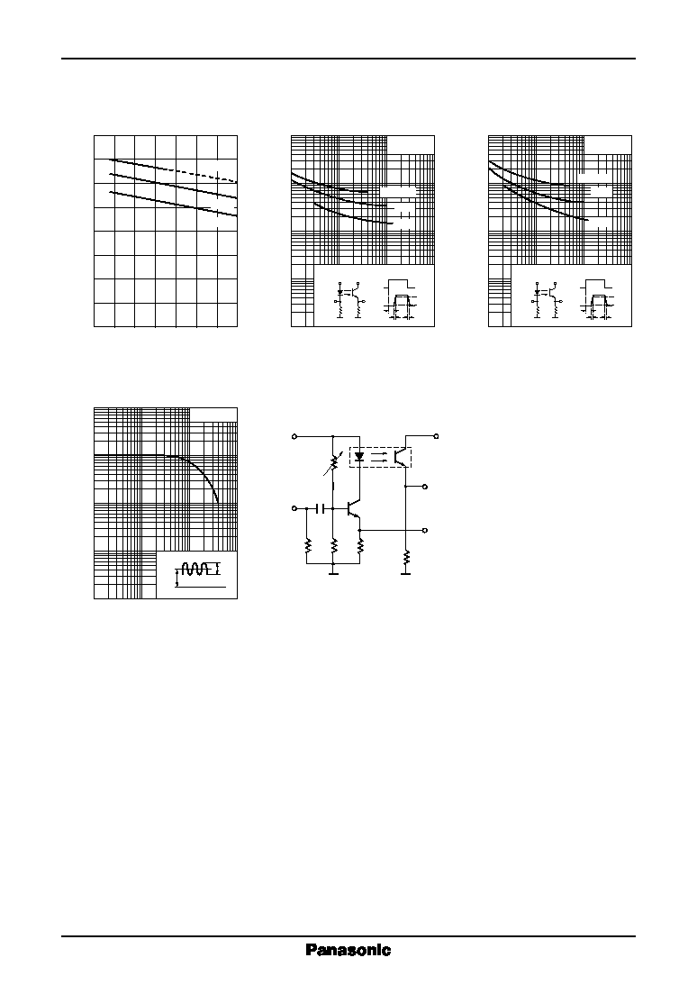
t
r
-- I
C
10
1
Collector current I
C
(mA)
Rise time t
r
(
µ
s)
1
10
10
≠2
10
≠1
10
≠1
10
2
10
2
V
CC
= 10V
Ta = 25∞C
t
f
-- I
C
Collector current I
C
(mA)
Fall time t
f
(
µ
s)
10
1
10
≠2
10
≠1
10
2
1
10
10
≠1
10
2
V
CC
= 10V
Ta = 25∞C
V
F
-- Ta
1.6
1.2
0.8
0.4
Ambient temperature Ta (∞C )
Forward voltage V
F
(V)
0
20
40
60
80
100
0
≠ 40 ≠ 20
Frequency characteristics
Measurement circuit of
frequency characteristics
10
1
Frequency f (kHz)
Relative power output P (dB)
10
10
2
10
3
10
≠3
10
≠1
10
≠2
1
Ta = 25∞C
R
L
= 1k
500
100
R
L
= 1k
500
100
10mA
1mA
I
F
= 50mA
10%
90%
t
d
t
r
t
f
R
L
V
CC
Sig.
OUT
Sig.
OUT
50
Sig.IN
;;
;;
;
;
10%
90%
t
d
t
r
t
f
R
L
V
CC
Sig.
OUT
Sig.
OUT
50
Sig.IN
;;
;
I
F
= 5mA
2mA
;;
;
;;
;
;
;
50k
50
50
5k
50
+10V
+10V
Sig.OUT
Sig.OUT
Sig.IN ≠
+
100
µ
F
16V
Caution for Safety
DANGER
Please read the following notes before using the datasheets
A. These materials are intended as a reference to assist customers with the selection of Panasonic semiconduc-
tor products best suited to their applications.
Due to modification or other reasons, any information contained in this material, such as available product
types, technical data, and so on, is subject to change without notice.
Customers are advised to contact our semiconductor sales office and obtain the latest information before
starting precise technical research and/or purchasing activities.
B. Panasonic is endeavoring to continually improve the quality and reliability of these materials but there is always
the possibility that further rectifications will be required in the future. Therefore, Panasonic will not assume any
liability for any damages arising from any errors etc. that may appear in this material.
C. These materials are solely intended for a customer's individual use.
Therefore, without the prior written approval of Panasonic, any other use such as reproducing, selling, or
distributing this material to a third party, via the Internet or in any other way, is prohibited.
Request for your special attention and precautions in using the technical information
and semiconductors described in this material
(1) An export permit needs to be obtained from the competent authorities of the Japanese Government if any of the
products or technologies described in this material and controlled under the "Foreign Exchange and Foreign
Trade Law" is to be exported or taken out of Japan.
(2) The technical information described in this material is limited to showing representative characteristics and
applied circuit examples of the products. It does not constitute the warranting of industrial property, the granting
of relative rights, or the granting of any license.
(3) The products described in this material are intended to be used for standard applications or general electronic
equipment (such as office equipment, communications equipment, measuring instruments and household ap-
pliances).
Consult our sales staff in advance for information on the following applications:
∑ Special applications (such as for airplanes, aerospace, automobiles, traffic control equipment, combustion
equipment, life support systems and safety devices) in which exceptional quality and reliability are required,
or if the failure or malfunction of the products may directly jeopardize life or harm the human body.
∑ Any applications other than the standard applications intended.
(4) The products and product specifications described in this material are subject to change without notice for
reasons of modification and/or improvement. At the final stage of your design, purchasing, or use of the prod-
ucts, therefore, ask for the most up-to-date Product Standards in advance to make sure that the latest specifi-
cations satisfy your requirements.
(5) When designing your equipment, comply with the guaranteed values, in particular those of maximum rating, the
range of operating power supply voltage and heat radiation characteristics. Otherwise, we will not be liable for
any defect which may arise later in your equipment.
Even when the products are used within the guaranteed values, redundant design is recommended, so that
such equipment may not violate relevant laws or regulations because of the function of our products.
(6) When using products for which dry packing is required, observe the conditions (including shelf life and after-
unpacking standby time) agreed upon when specification sheets are individually exchanged.
(7) No part of this material may be reprinted or reproduced by any means without written permission from our
company.
Gallium arsenide material (GaAs) is used
in this product.
Therefore, do not burn, destroy, cut, crush, or chemi-
cally decompose the product, since gallium arsenide
material in powder or vapor form is harmful to human
health.
Observe the relevant laws and regulations when dispos-
ing of the products. Do not mix them with ordinary in-
dustrial waste or household refuse when disposing of
GaAs-containing products.
2001 MAR