 | –≠–ª–µ–∫—Ç—Ä–æ–Ω–Ω—ã–π –∫–æ–º–ø–æ–Ω–µ–Ω—Ç: DN6848 | –°–∫–∞—á–∞—Ç—å:  PDF PDF  ZIP ZIP |

Hall ICs
1
Publication date: November 2002
SPC00003CEB
DN6848SE
DN6848S
DN6848/SE/S
Wide operating temperature range
(
-40∞C to +100∞C)
One-way magnetic field operation
Overview
In each of Hall ICs, a Hall element, an amplifier circuit,
a Schmidt circuit, a stabilized power supply, and a tem-
perature compensation circuit are integrated on a single
chip by IC technique. The Hall element output is ampli-
fied by the amplifier circuit, and converted into the corre-
sponding digital signals through the Schmidt circuit so
that TTL and MOS IC are directly drivable.
Features
∑ High sensitivity and low drift
∑ Stabilized temperature characteristics owing to addi-
tional integration of temperature compensation circuit.
∑ Wide operating supply voltage range
(V
CC
= 4.5 V to 16 V)
∑ One-way magnetic field operation
∑ TTL and MOS IC are directly drivable by the output.
∑ Open collector output
Applications
∑ Speed sensor, position sensor, rotation sensor, keyboard
switch, micro switch and the like
Block Diagram (DN6848/SE/S)
Note) The number in ( ) shows the pin number for the DN6848S.
SSIP003-P-0000A
Unit: mm
SSIP003-P-0000C
Unit: mm
Unit: mm
4.52±0.3
0.55±0.15
0.4±0.1
1.54±0.1
1.27
1 2 3
(0.4)
12.5±06.5
(0.72)
4.52±0.3
(1.0)
(1.0)
1 2 3
5
∞
(5
∞)
2
∞
1.27
4.0±0.2
(1.0)
(1.0)
(0.7)
4.5±0.2
0.43
+0.1
≠0.05
0.43
+0.1
≠0.05
0.55±0.15
2.0±0.2
0.8±0.1
(1.0)
10.5±0.5
ESOP004-P-0200
1.6
3.0±0.3
0.6±0.2
1
2
4
3
5.4±0.4
3.0±0.3
1.5±0.3
0.4±0.2
0.1±0.1
0.2
0.95±0.2
0.4±0.15
+0.15 ≠0.05
1 : V
CC
2 : GND
3 : Output
1 : V
CC
2 : GND
3 : Output
1 : V
CC
2 : N.C. or GND
3 : Output
4 : GND
DN6848
Power supply circuit and
temperature compensation circuit
1
V
CC
2
GND
(4)
N.C.
or
GND
(2)
3
Output
Hall element Amplifier Schmidt
trigger
Output stage
Note) The packages (SSIP003-P-0000A, SSIP003-P-
0000C and ESOP004-P-0200) of this product
will be changed to lead-free type (SSIP003-P-
0000H, SSIP003-P-0000J and ESOP004-P-
0200A). See the new package dimensions sec-
tion later of this datasheet.

DN6848/SE/S
2
SPC00003CEB
Recommended Operating Range
Parameter
Symbol
Range
Unit
Supply voltage
V
CC
4.5 to 16
V
Absolute Maximum Ratings
Parameter
Symbol
Rating
Unit
Supply voltage
V
CC
18
V
Supply current
I
CC
8
mA
Circuit current
I
O
20
mA
Power dissipation
P
D
150
mW
Operating ambient temperature
T
opr
-40 to +100
∞C
Storage temperature
T
stg
-55 to +125
∞C
Note) 1. The variation of operating magnetic flux density does not depend on supply voltage due to its built-in stabilized power
source. (V
CC
should be confined to the range of 4.5 V to 16 V.)
2. A supply current increases by approximately 1 mA when its output level varies from high to low.
Electrical Characteristics at T
a
= 25∞C
Parameter
Symbol
Conditions
Min
Typ
Max
Unit
Operating magnetic flux density
B
1(L-H)
V
CC
= 12 V
0.5
9
21
mT
B
2(H-L)
V
CC
= 12 V
1.5
11
22
mT
Hysteresis width
BW
V
CC
= 12 V
1
2
mT
Output voltage
V
OL
V
CC
= 16 V, I
O
= 12 mA, B = 22 mT
0.4
V
V
CC
= 4.5 V, I
O
= 12 mA, B = 22 mT
0.4
V
Output current
I
OH
V
CC
= 4.5 V to 16 V, V
O
= 16 V,
10
µA
B
= 0 mT
Supply current
I
CC
V
CC
= 16 V
6
mA
V
CC
= 4.5 V
5.5
mA
Technical Data
∑ Position of Hall element (unit: mm)
A Hall element is placed on the shaded part in the figure.
DN6848
DN6848SE
DN6848S
Distance from package surface to sensor part
0.7
0.42
0.65
1.0
1.0
1.5
1.5
1.0 1.63
1.0
1.25
1.0 1.75
1.0
1.3
Note) This IC is not suitable for car electrical equipment.
DN6848/SE/S
3
SPC00003CEB
Technical Data (continued)
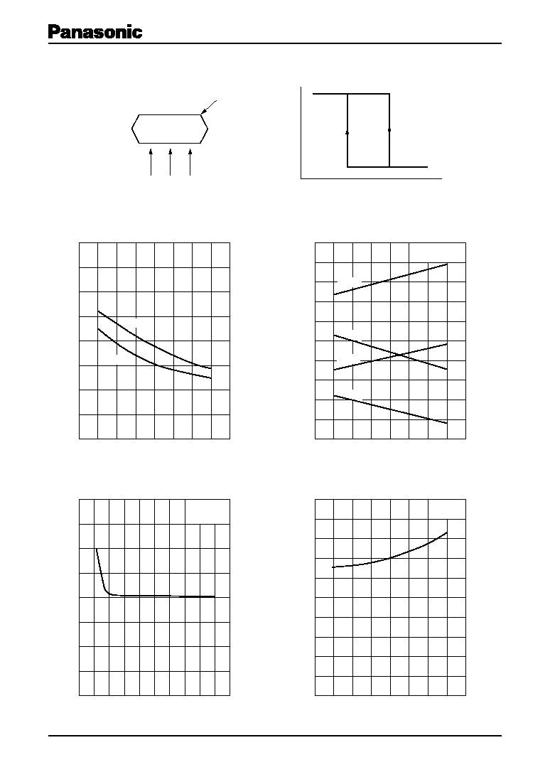
∑ Magneto-electro conversion characteristics
Applying direction of magnetic flux
Marked face
B
H-L
B
L-H
Magnetic flux density B
Output v
oltage
V
O
∑ Main characteristics
Supply current
Ambient temperature
Operating magnetic flux density
Ambient temperature
0
125
V
CC
= 12 V
I
O
= 12 mA
0
1
2
3
4
5
6
7
8
2.5
5.0
7.5
10.0
12.5
15.0
17.5
20.0
-50
-25
0
25
50
75
100
125
-50
-25
0
25
50
75
100
2.5
7.5
12.5
17.5
22.5
5.0
10.0
15.0
20.0
25.0
125
-50
-25
0
25
50
75
100
10
20
30
40
50
60
70
80
90
100
0
20
2
4
6
8
10
12
14
16
18
Sample 3
Sample 2
Sample 4
Sample 1
V
CC
= 4.5 V 16 V
B
H-L
V
CC
= 16 V
V
CC
= 4.5 V
T
a
= 25∞C
Ambient temperature T
a
(∞C)
Operating magnetic flux density B (mT)
Ambient temperature T
a
(∞C)
Supply current I
CC
(mA)
Ambient temperature T
a
(∞C)
Lo
w-le
v
el output v
oltage
V
OL
(mV)
Supply voltage V
CC
(V)
Operating magnetic flux density B (mT)
Operating magnetic flux density
Supply voltage
Low-level output voltage
Ambient temperature
DN6848/SE/S
4
SPC00003CEB
Caution on Use of Hall ICs
The Hall ICs are often used to detect movement. In such cases, the position of the Hall IC may be changed by
exposition to shock or vibration over a long period of time, and it causes the detection level change. To prevent this, fix
the package with adhesives or fix it on a dedicated case.
1. A case using an adhesive
Some kinds of adhesive generate corrosive gas (such as chloric gas) during curing. This corrosive gas corrodes
the aluminum on the surface of the Hall IC, and may cause a functional defect of disconnection.
If Hall IC is to be sealed after installation, attention should be given to the adhesive or resin used for peripherals
and substrate cleaner, as well as to the adhesive used for Hall IC installation. Please confirm the above matter to those
manufacturers before using.
We could not select the specified adhesive, for we find it difficult to guarantee the ingredient of each adhesive.
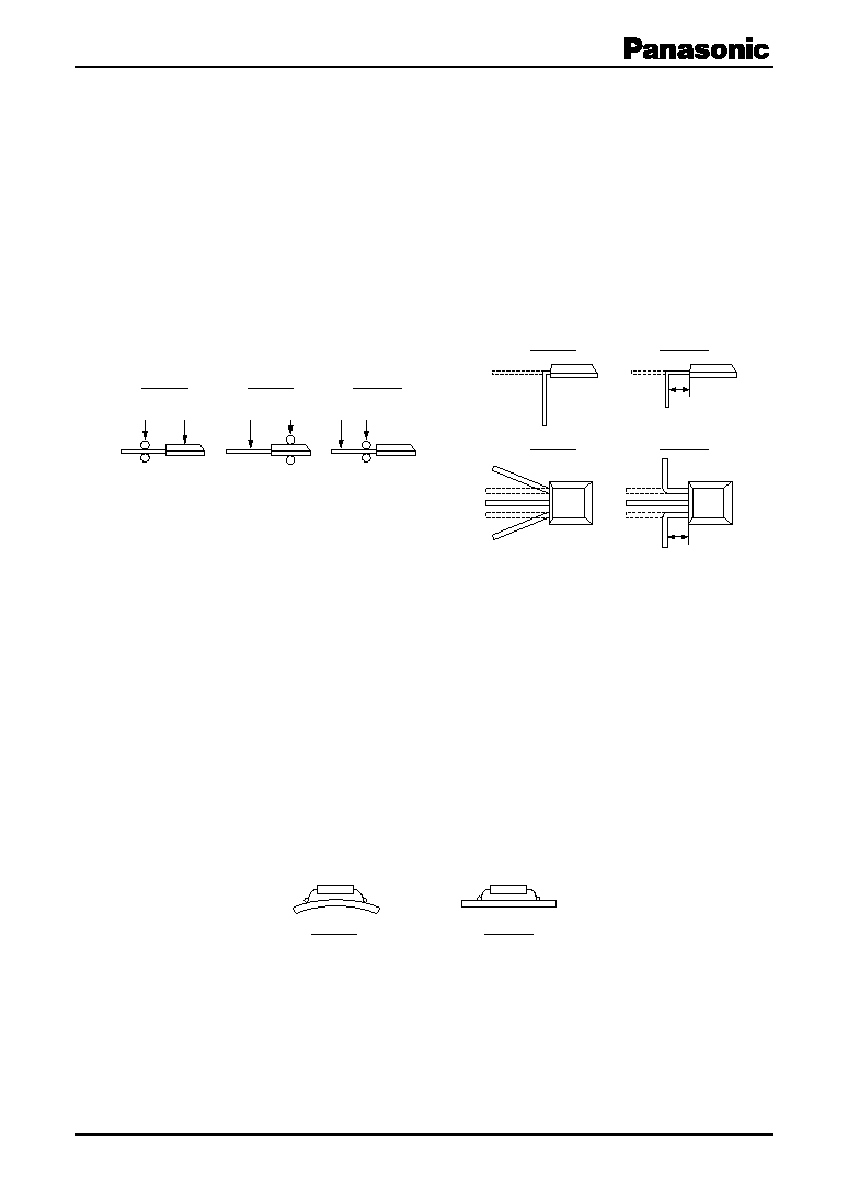
2. A case bending lead wire
Bend the lead wire without stressing the package.
3. Power supply line/Power transmission line
If a power supply line/power transmission line becomes longer, noise and/or oscillation may be found on the
line. In this case, set the capacitor of 0.1
µF to 10 µF near the Hall IC to prevent it.
If a voltage of 18 V or more is thought to be applied to the power supply line (flyback voltage from coil or the
ignition pulse, etc.), avoid it with external components (capacitor, resistor, Zener diode, diode, surge absorbing ele-
ments, etc.).
4. On mounting of the surface mount type package (ESOP004-P-0200)
Set pin 2 of the ESOP004-P-0200 package open, or connect it to GND. The IC will be damaged if it is connected
to V
CC
.
When mounted on the printed circuit board, the Hall IC may be highly stressed by the warp that may occur from
the soldering. This may also cause a change in the operating magnetic flux density and a deterioration of its resistance
to moisture.
5. V
CC
and GND
Do not reverse V
CC
and GND. If the V
CC
and GND pins are reversely connected, this IC will be destroyed. If the
IC GND-pin voltage is set higher than other pin voltage, the IC configuration will become the same as a forward
biased diode. Therefore, it will turn on at the diode forward voltage (approximately 0.7 V), and a large current will
flow through the IC, ending up in its destruction. (This is common to monolithic IC.)
6. Cautions on power-on of Hall IC
When a Hall IC is turned on, the position of the magnet or looseness may change the output of a Hall IC, and a pulse
may be generated. Therefore, care should be given whenever the output state of a Hall IC is critical when the supply
power is on.
Fixed
W
Fixed
Correct
(a)
(b)
Fixed
Bending method of lead wire
Bending position of lead wire
W
W
3 mm *
3 mm *
*: The distance can be within 3 mm, if no stress is applied
to the resin mold by tightly fixing the lead wires with a
metallic mold or the like.
Wrong
Correct
Wrong
Correct
Wrong
Wrong
Correct
Wrong

DN6848/SE/S
5
SPC00003CEB
Caution on Use of Hall ICs (continued)
7. Fixing a Hall IC
When the Hall IC of an insertion type package installed by soldering the lead wire only is to be used under
vibration, fix it firmly with a holder. Otherwise, vibration may cause metal fatigue in the lead wire of Hall IC,
resulting in wire breakage.
8. On fixing a Hall IC to holder
When a Hall IC is mounted on the printed circuit board with a holder and the coefficient of expansion of the holder
is large, the lead wire of the Hall IC will be stretched and it may give a stress to the Hall IC.
If the lead wire is stressed intensely due to the distortion of holder or board, the adhesives between the package
and the lead wire may be weakened and cause a minute gap resulting in the deterioration of its resistance to moisture.
Sensitivity may also be changed by this stress.
9. On using flux in soldering
Choose a flux which does not include ingredients from halogen group, such as chlorine, fluorine, etc. The
ingredients of halogen group may enter where the lead frame and package resin joint, causing corrosion and the
disconnection of the aluminum wiring on the surface of an IC chip.
10. In case of the magnetic field of a magnet is too strong
Output may be inverted when applying a magnetic flux density of 100 mT or more. Accordingly, magnetic flux
density should be used within the range of 100 mT.
11. On mounting , deburring and soldering of insertion type package
If the leads of a Hall IC in an insertion type package are inserted up to their root part through holes on the printed
circuit board, abnormal stress is applied to the package and the reliability of the Hall IC is likely to deteriorate. So,
when mounting each Hall IC of the insertion type, insert the leads in due degree at which the bottom face of the
package is separated at least 2 mm from the top face of the PCB.
Also note that burrs of epoxy resin may be left sticking to the lead wires. (We are trying to remove such burrs as
much as possible in the deburring process, but in some cases, they are not perfectly removable.)
12. On surface treatment of mini-mold package
Surface treatment is available in either smooth or dull finish.
13. On soldering of the surface mount type package
Surface mounting type Hall ICs are apt to change its electrical characteristics due to the stress from soldering at
mounting. Therefore, avoid the mounting by flow (dipping) and a soldering iron. Please mount it by reflow soldering
abiding by its recommended conditions.
2 mm
Printed board
Remaining burrs
When soldering the leads, remenber to separate
the soldering position by 2 mm or more from
the resin part of the package.