Äîêóìåíòàöèÿ è îïèñàíèÿ www.docs.chipfind.ru
Chip Resistor Array
Design and specifi cations are each subject to change without notice. Ask factory for the current technical specifi cations before purchase and/or use.
Should a safety concern arise regarding this product, please be sure to contact us immediately.
E
1
X
2
B
3
V
4
8
5
V
6
4
7
7
8
2
9
J
10
V
11
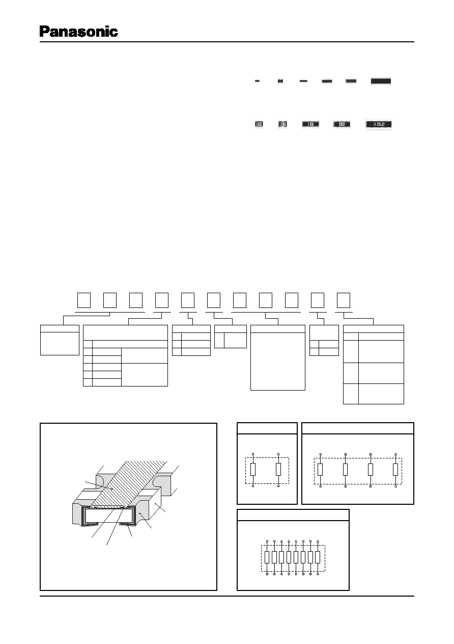
Thick Film
Chip Resistor
Networks
Chip Resistor Array
Type: inches
Product Code
0201 Array
0402 Array
0603 Array
0402 Array
0603 Array
0805 Array
1
2
3
N
V
S
4
8
H
4 Terminal
8 Terminal
16 Terminal
No. of Terminal
Schematics
V
Isolated
type
The first two digits are
significant figures of
resistance value and
the third one denotes
the number of zeros
following. Jumper is
expressed by R00
Resistance Value
Example: 222: 2.2 k
Resistance
Tolerance
J
0
±5 %
Jumper
Packaging Methods
Code
Nil
X
V
Embossed
Carrier Taping
(S8V)
Punched Carrier Taping
2 mm pitch
(14V, 18V, 24V, 28V, N8V)
Punched Carrier Taping
4 mm pitch
(2HV, 34V, 38V, V4V, V8V)
Convex Terminal
Concave Terminal
Packaging
Protective coating
Thick film
resistive element
Electrode (Inner)
Electrode (Between)
Electrode (Outer)
Alumina substrate
4
3
1
2
8
1
7
2
6
3
5
4
16
1
15
2
14
3
13
4
12
5
11
6
10
7
9
8
Construction (Example : Concave Terminal)
Schematics
Isolated type
14V, 24V, 34V, V4V
18V, 28V, N8V, 38V, V8V, S8V
2 resistors
4 resistors
2HV
8 resistors
Features
High density
2 resistors in 0.8 mm
0.6 mm size (EXB14V)
4 resistors in 1.4 mm
0.6 mm size (EXB18V)
2 resistors in 1.0 mm
1.0 mm size (EXB24V)
4 resistors in 2.0 mm
1.0 mm size (EXB28V, N8V)
8 resistors in 3.8 mm
1.6 mm size (EXB2HV)
2 resistors in 1.6 mm
1.6 mm size (EXB34V, V4V)
4 resistors in 3.2 mm
1.6 mm size (EXB38V, V8V)
4 resistors in 5.1 mm
2.2 mm size (EXBS8V)
Improvement of placement effi ciency
Placement effi ciency of Chip Resistor Array is two, four or eight times of the fl at type chip resistor
Type:
EXB1 : 0201 Array
EXB2 : 0402 Array
EXB3 : 0603 Array
EXBN : 0402 Array
EXBV : 0603 Array
EXBS : 0805 Array
Explanation of Part Numbers
Chip Resistor Array
May. 2005
Design and specifi cations are each subject to change without notice. Ask factory for the current technical specifi cations before purchase and/or use.
Should a safety concern arise regarding this product, please be sure to contact us immediately.
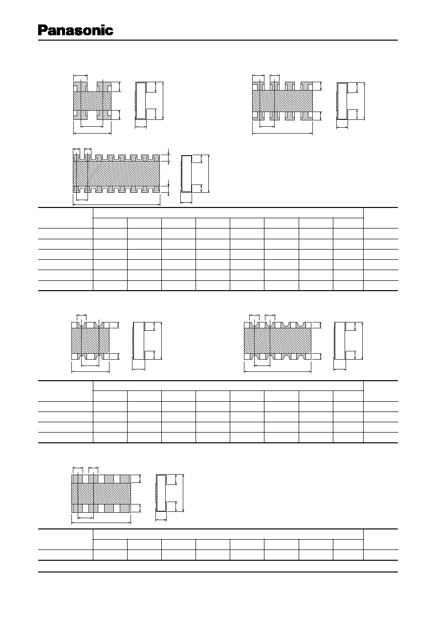
Chip Resistor Array
P
P
L
L
G
G
G
W
G
B
B
W
B
B
A1
A1
A2
EXBV4V
EXBN8V, V8V, S8V
T
T
P
L
T
G
W
G
B
B
A1
A2
EXB18V
A1
P
T
P
L
T
L
BB
G
BB
GG
W
W
G
A1
A2
EXB14V, 24V, 34V
EXB28V, 38V
P
T
L
G
W
G
BB
A1
A2
EXB2HV
Type
(inches)
Dimensions (mm)
Mass (Weight)
[g/1000 pcs.]
L
W
T
A1
A2
B
P
G
EXBN8V (0402 4)
2.00
±0.10
1.00
±0.10
0.45
±0.10
0.30
±0.10
0.30
±0.10
0.20
±0.15
(0.50)
0.30
±0.15
3.0
EXBV4V (0603 2)
1.60
+0.20
1.60
+0.20
0.60
±0.10
0.60
±0.10
--
0.30
±0.15
(0.80)
0.45
±0.15
5.0
EXBV8V (0603 4)
3.20
+0.20
1.60
+0.20
0.60
±0.10
0.60
±0.10
0.60
±0.10
0.30
±0.15
(0.80)
0.45
±0.15
10
EXBS8V (0805 4)
5.08
+0.20
2.20
+0.20
0.70
±0.20
0.80
±0.15
0.80
±0.15
0.50
±0.15
(1.27)
0.55
±0.15
30
Type
(inches)
Dimensions (mm)
Mass (Weight)
[g/1000 pcs.]
L
W
T
A1
A2
B
P
G
EXB14V (0201 2)
0.80
±0.10
0.60
±0.10
0.35
±0.10
0.35
±0.10
--
0.15
±0.10
(0.50)
0.15
±0.10
0.5
EXB24V (0402 2)
1.00
±0.10
1.00
±0.10
0.35
±0.10
0.40
±0.10
--
0.18
±0.10
(0.65)
0.25
±0.10
1.2
EXB28V (0402 4)
2.00
±0.10
1.00
±0.10
0.35
±0.10
0.45
±0.10
0.35
±0.10
0.20
±0.10
(0.50)
0.25
±0.10
2.0
EXB2HV (0402 8)
3.80
±0.10
1.60
±0.10
0.45
±0.10
0.35
±0.10
0.35
±0.10
0.30
±0.10
(0.50)
0.30
±0.10
9.0
EXB34V (0603 2)
1.60
±0.20
1.60
±0.15
0.50
±0.10
0.65
±0.15
--
0.30
±0.20
(0.80)
0.30
±0.20
3.5
EXB38V (0603 4)
3.20
±0.20
1.60
±0.15
0.50
±0.10
0.65
±0.15
0.45
±0.15
0.30
±0.20
(0.80)
0.35
±0.20
7.0
0.10
0.10
0.10
0.10
0.10
0.10
Type
(inches)
Dimensions (mm)
Mass (Weight)
[g/1000 pcs.]
L
W
T
A1
A2
B
P
G
EXB18V (0201 4)
1.40
±0.10
0.60
±0.10
0.35
±0.10
0.20
±0.10
0.20
±0.10
0.10
±0.10
(0.40)
0.20
±0.10
1.0
( ) Reference
Dimensions in mm (not to scale)
(1) Convex Terminal type
(2) Concave Terminal type
(3) Flat Terminal type
( ) Reference
( ) Reference
May. 2005
Chip Resistor Array
Design and specifi cations are each subject to change without notice. Ask factory for the current technical specifi cations before purchase and/or use.
Should a safety concern arise regarding this product, please be sure to contact us immediately.
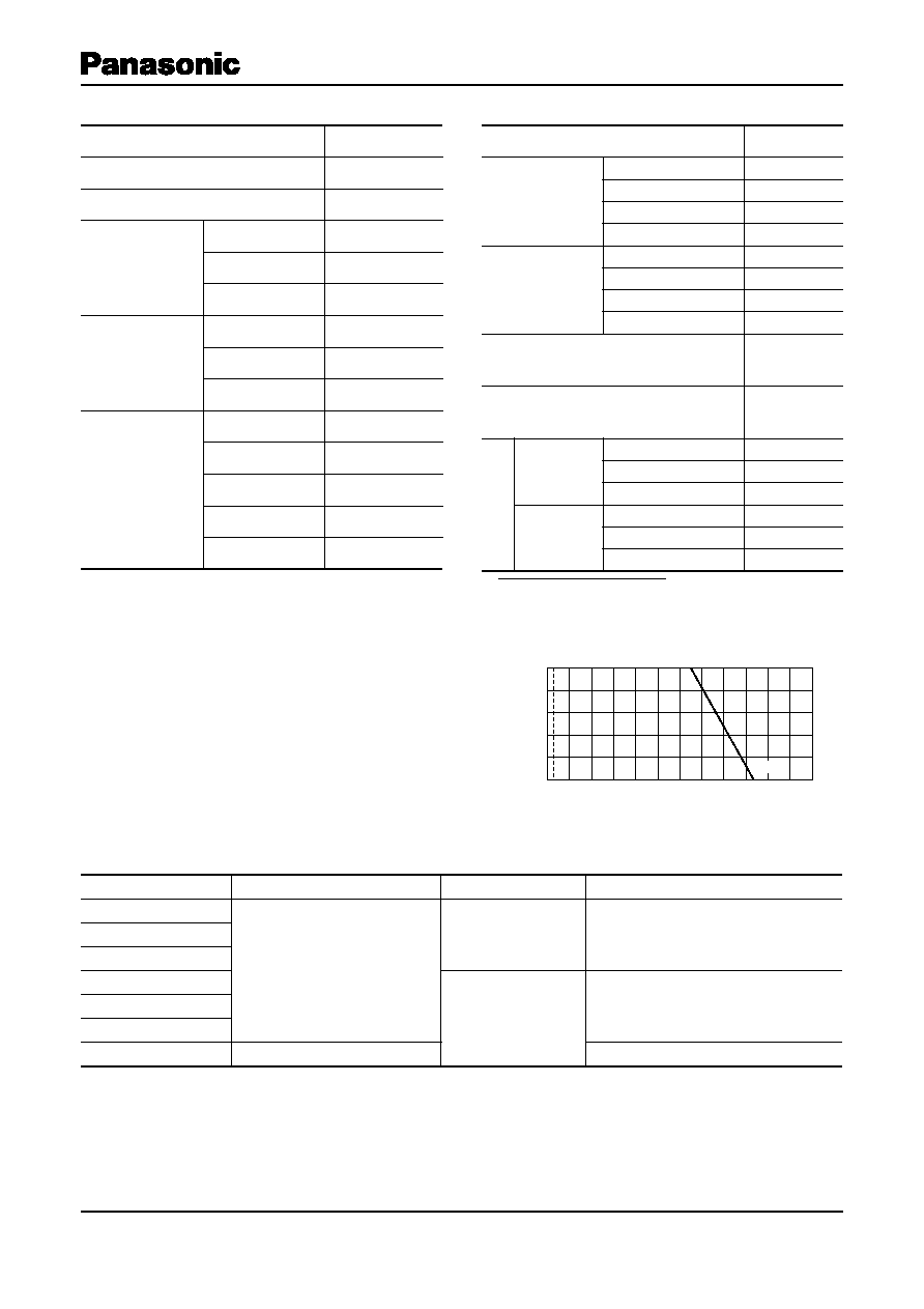
60 40 20
0
20 40 60 80 100 120 140 160 180
0
20
40
60
80
100
70
°C
55
°C
125
°C
Ambient Temperature (
°C)
Rated
Load
(%)
Item
Specifi cations
Resistance Range
10 to 1 M :E24 series
Resistance Tolerance
J: ±5 %
Number of Terminals
14V,24V,V4V,34V
4 terminal
18V,28V,N8V,38V,V8V,S8V 8 terminal
2HV
16 terminal
Number of Resistors
14V,24V,V4V,34V
2 terminal
18V,28V,N8V,38V,V8V,S8V 4 terminal
2HV
8 terminal
Power Rating at 70 °C
14V,28V,N8V
0.031 W/element
18V
0.031 W/element
(0.1 W/package)
24V,V4V,34V,V8V,38V
0.063 W/element
S8V
0.1 W/element
2HV
0.063 W/element
(0.25 W/package)
Type
Kind of Taping
Pitch (P
1
)
Quantity
EXB14V, 18V
Punched Carrier Taping
2 mm
10000 pcs./reel
EXB24V, 28V
EXBN8V
EXB2HV
4 mm
5000 pcs./reel
EXB34V, 38V
EXBV4V, V8V
EXBS8V
Embossed Carrier Taping
2500 pcs./reel
Ratings
(1) Rated Continuous Working Voltage (RCWV) shall be de ter mined from RCWV= Power Rating
Resistance Value, or Limiting Element Voltage (max.
RCWV) listed above, whichever less.
(2) Overload (Short-time Overload) Test Voltage (SOTV) shall be determined from SOTV=2.5
Power Rating or max. Overload (Voltage) list ed above whichever less.
Power Derating Curve
For resistors operated in ambient temperature above
70 °C, power rating shall be derated in accordance
with the fi gure on the right.
Packaging Methods (Taping)
Standard Quantity
Item
Specifi cations
Limiting Element Voltage
(1)
Max. Rated Continuous
Working Voltage
14V,18V
12.5 V
2HV
25 V
24V,28V,N8V,38V,34V,V4V,V8V 50 V
S8V
100 V
Max. Over-load Voltage
(2)
14V,18V
25 V
2HV
50 V
24V,28V,N8V,38V,34V,V4V,V8V 100 V
S8V
200 V
T.C.R.
±200 10
-6
/°C(ppm/°C)
Category Temperature Range
(Operating Temperature Range)
55 °C to 125 °C
Jump
er
A
r
r
a
y
Rated Current
14V,18V
0.5 A
2HV,24V,28V,N8V,38V,34V,V4V,V8V 1 A
S8V
2 A
Max, Overload Current
14V,18V
1 A
2HV,24V,28V,N8V,38V,34V,V4V,V8V 2 A
S8V
4 A
( )
Sep. 2005
Design and specifi cations are each subject to change without notice. Ask factory for the current technical specifi cations before purchase and/or use.
Should a safety concern arise regarding this product, please be sure to contact us immediately.
Chip Resistor Array
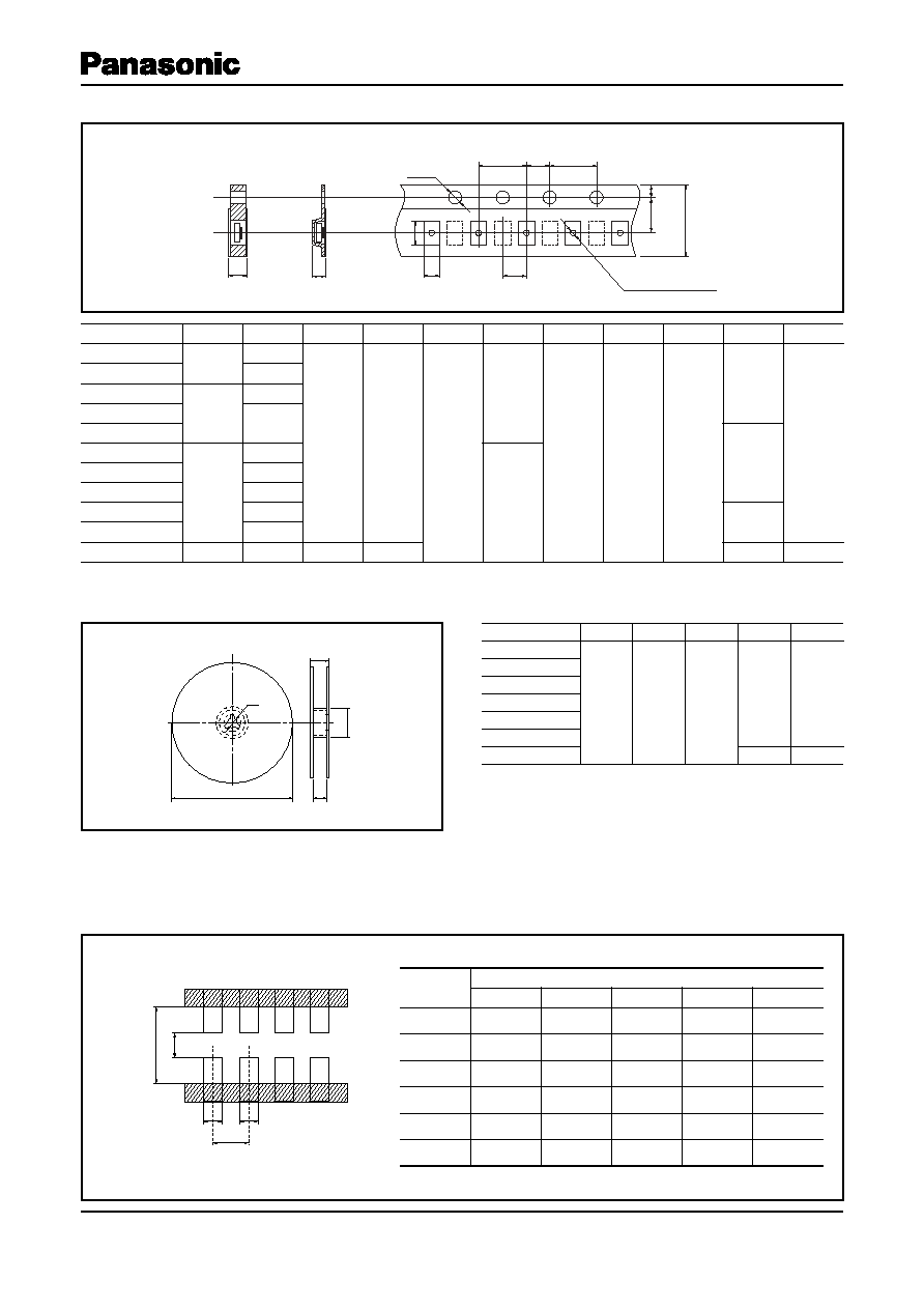
T
T
A
P
0
P
2
P
1
P
1
fD
0
B
F
W
E
fD
1
(Only Emboss)
(2 mm pitch)
f
B
W
T
fA
fC
f
a
b
c
p
Type
A
B
W
F
E
P
1
P
2
P
0
fD
0
T
fD
1
EXB14V
0.70
+0.10
0.90
+0.10
8.00
±0.20
3.50
±0.05
1.75
±0.10
2.00
±0.10
2.00
±0.05
4.00
±0.10
1.50
+0.10
0.52
±0.05
_
EXB18V
1.60
±0.10
EXB24V
1.20
±0.10
1.20
±0.10
EXB28V
2.20
±0.10
EXBN8V
0.70
±0.05
EXB2HV
1.95
±0.15
4.10
±0.15
4.00
±0.10
EXB34V
1.95
±0.20
EXB38V
3.60
±0.20
EXBV4V
1.95
±0.20
0.84
±0.05
EXBV8V
3.60
±0.20
EXBS8V
2.80
±0.20
5.70
±0.20
12.00
±0.30
5.50
±0.20
1.60 max. 1.50
+0.10
Type
fA
fB
fC
W
T
EXB14V,18V
180.0
+0
60 min.
13.0
±1.0
9.0
±1.0
11.4
±1.0
EXB24V,28V
EXBN8V
EXB2HV
EXB34V,38V
EXBV4V,V8V
EXBS8V
13.0
±1.0
15.4
±2.0
3.0
0
0
0.05
0.05
Type
Dimensions
Unit (mm)
a
b
c
p
f
14V
0.20 to 0.30 0.25 to 0.30 0.25 to 0.30
0.50
0.80 to 0.90
18V
0.20 to 0.30 0.15 to 0.20 0.15 to 0.20
0.40
0.80 to 0.90
24V
0.5
0.35 to 0.40 0.35 to 0.40
0.65
1.4 to 1.5
V4V,V8V
0.7 to 0.9
0.4 to 0.45
0.4 to 0.45
0.80
2 to 2.4
34V,38V
0.7 to 0.9
0.4 to 0.5
0.4 to 0.5
0.80
2.2 to 2.6
S8V
1 to 1.2
0.5 to 0.75
0.5 to 0.75
1.27
3.2 to 3.8
Punched Carrier Embossed Carrier
Carrier Tape
Taping Reel
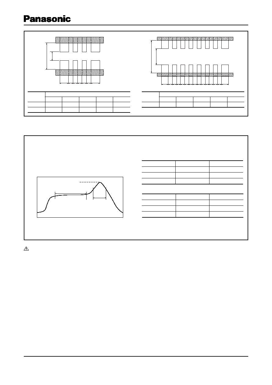
Land pattern design
Recommended land pattern design for Network chip is shown below.
Unit (mm)
Unit (mm)
(Not to scale)
Sep. 2005
Chip Resistor Array
Design and specifi cations are each subject to change without notice. Ask factory for the current technical specifi cations before purchase and/or use.
Should a safety concern arise regarding this product, please be sure to contact us immediately.
Preheating
Peak
Heating
Temperature
Time
b
b
d
d
d
d
d
d
d
c
c
c
c
c
c
a
f
f
a
b
d
b
c
c
d
d
Temperature
Time
Preheating
140 °C to 160 °C
60 s to 120 s
Main heating
Above 200 °C
30 s to 40 s
Peak
235 ± 5 °C
max. 10 s
Temperature
Time
Preheating
150 °C to 180 °C
60 s to 120 s
Main heating
Above 230 °C
30 s to 40 s
Peak
max. 260 °C
max. 10 s
Recommended Soldering Conditions
Recommendations and precautions are described below.
Recommended soldering conditions for refl ow
For soldering (Example : Sn/Pb)
For lead-free soldering (Example : Sn/Ag/Cu)
Safety Precautions
· We do not recommend fl ow soldering, because a solder bridge may form.
Flow soldering
Type
Dimensions
Unit (mm)
a
b
c
d
f
28V
0.40
0.525
0.25
0.25
1.40
N8V
0.45 to 0.50 0.35 to 0.38
0.25
0.25
1.40 to 2.00
Type
Dimensions
Unit (mm)
a
b
c
d
f
2HV
1.00
0.425
0.25
0.25
2.00
(Not to scale)
(Not to scale)
The following are precautions for individual products. Please also refer to the precautions common to Fixed Resistors
shown on page ER3 of this catalog.
1. Take measures against mechanical stress during and after mounting of Chip Resistor Array (hereafter called the
resistors) so as not to damage their electrodes and protective coatings.
Be careful not to misplace the resistors on the land patterns. Otherwise, solder bridging may occur.
2. If a transient load (heavy load in a short time) like a pulse is expected to be applied, check and eval u ate the op er a tions
of the resistors when installed in your products before use.
Never exceed the rated power. Otherwise, the performance and/or reliability of the resistors may be impaired.
3. Do not use halogen-based or other high-activity fl ux. Otherwise, the residue may impair the resistors' per for mance
and/or reliability.
4. When soldering with a soldering iron, never touch the resistors' bodies with the tip of the soldering iron. When using a
soldering iron with a high temperature tip, fi nish soldering as quickly as possible (within three seconds at 350 °C max.).
5. As the amount of applied solder becomes larger, the mechanical stress applied to the resistors increases, causing
problems such as cracks and faulty characteristics. Avoid applying an excessive amounts of solder.
6. Do not apply shock to the resistors or pinch them with a hard tool (e.g. pliers and tweezers). Oth er wise, the re sis tors'
protective coatings and bodies may be chipped, affecting their performance.
7. Avoid excessive bending of printed circuit boards in order to protect the resistors from abnormal stress.
· Refl ow soldering shall be performed a maximum of
two times.
· Please contact us for additional information when
used in conditions other than those specifi ed.
· Please measure the temperature of the terminals
and study every kind of solder and printed circuit
board for solderability be fore ac tu al use.
Mar. 2005