
PAGE 1
Part Number: SD620CS - SD6100CS
SD620CS Thru SD6100CS
DPAK SURFACE MOUNT SCHOTTKY BARRIER RECTIFIER
VOLTAGE - 20 to 100 Volts CURRENT - 6.0 Amperes
FEATURES
∑ Plastic package has Underwriters Laboratory Flammability
Classification 94V-O
∑ For surface mounted applications
∑ Low profile package
∑ Built-in strain relief
∑ Metal to silicon rectifier majority carrier conduction
∑ Low power loss, High efficiency
∑ High current capability, low V
F
∑ High surge capacity
∑ For use in low voltage high frequency inverters, free wheeling, and
polarity protection applications
∑ High temperature soldering guaranteed:260∞C/10 seconds at terminals
MECHANICAL DATA
Case: D PAK/TO-252 molded plastic
Terminals: Solder plated, solderable per MIL-STD-750,Method 2026
Polarity: Color band denotes cathode
Standard packaging: 16mm tape (EIA-481)
Weight: 0.015 ounce, 0.4 gram.
MAXIMUM RATINGS AND ELECTRICAL CHARACTERISTICS
Ratings at 25
o
C ambient temperature unless otherwise specified.
Resistive or inductive load.
NOTES:
1. Pulse Test with PW=300µsec, 2% Duty Cycle.
2. Mounted on P.C. Board with 14mm
2
(.013mm thick) copper pad areas.
4
3
2
1
.
2
2
5(
5
.
7)
.
2
0
9(
5
.
3)
.106(2.7)
.090(2.3)
.09
(2.3)
.09
(2.3)
.032(0.8)
.012(0.3)
.02(.5)
.071(1.8)
.051(1.3)
.
0
4
0(
1
.
0)
M
I
N
.
3
2
1
4
.264(6.7)
.248(6.3)
.216(5.5)
.200(5.1)
.
0
6
3(
1
.
6)
.
0
4
7(
1
.
2)
.098(2.5)
.082(2.1)
.024(0.6)
.016(0.4)
DPAK / TO-252
S
L
O
B
M
Y
S
S
C
0
2
6
D
S
S
C
0
3
6
D
S
S
C
0
4
6
D
S
S
C
0
5
6
D
S
S
C
0
6
6
D
S
S
C
0
8
6
D
S
S
C
0
0
1
6
D
S
S
T
I
N
U
e
g
a
tl
o
V
e
s
r
e
v
e
R
k
a
e
P
t
n
e
r
r
u
c
e
R
m
u
m
i
x
a
M
V
RRM
0
2
0
3
0
4
0
5
0
6
0
8
0
0
1
s
tl
o
V
e
g
a
tl
o
V
S
M
R
m
u
m
i
x
a
M
V
RMS
4
1
1
2
8
2
5
3
2
4
6
5
0
7
s
tl
o
V
e
g
a
tl
o
V
g
n
i
k
c
o
l
B
C
D
m
u
m
i
x
a
M
V
DC
0
2
0
3
0
4
0
5
0
6
0
8
0
0
1
s
tl
o
V
t
n
e
r
r
u
C
d
e
if
it
c
e
R
d
r
a
w
r
o
F
e
g
a
r
e
v
A
m
u
m
i
x
a
M
T
t
a
C
5
7
=
o
C
I (
AV
)
0
.
6
0
.
6
0
.
6
0
.
6
0
.
6
0
.
6
0
.
6
s
p
m
A
t
n
e
r
r
u
C
e
g
r
u
S
d
r
a
w
r
o
F
k
a
e
P
n
o
d
e
s
o
p
m
ir
e
p
u
s
e
v
a
w
-
e
n
i
s
fl
a
h
e
l
g
n
i
s
s
m
3
.
8
)
d
o
h
t
e
m
C
E
D
E
J
(
d
a
o
l
d
e
t
a
r
I
FSM
5
7
5
7
5
7
5
7
5
7
5
7
5
7
s
p
m
A
A
0
.
3
t
a
e
g
a
tl
o
V
d
r
a
w
r
o
F
s
u
o
e
n
a
t
n
a
t
s
n
I
m
u
m
i
x
a
M
)
1
e
t
o
N
(
V
F
5
5
.
0
5
5
.
0
5
5
.
0
0
7
.
0
0
7
.
0
5
8
.
0
5
8
.
0
s
tl
o
V
T
)
1
e
t
o
N
(
t
n
e
r
r
u
C
e
s
r
e
v
e
R
C
D
m
u
m
i
x
a
M
A
5
2
=
o
C
T
e
g
a
tl
o
V
g
n
i
k
c
o
l
B
C
D
d
e
t
a
R
t
a
A
0
0
1
=
o
C
I
R
2
.
0
0
2
2
.
0
0
2
2
.
0
0
2
2
.
0
0
2
2
.
0
0
2
2
.
0
0
2
2
.
0
0
2
A
m
)
2
e
t
o
N
(
e
c
n
a
t
s
i
s
e
R
l
a
m
r
e
h
T
m
u
m
i
x
a
M
R
C
J
R
A
J
6
0
8
6
0
8
6
0
8
6
0
8
6
0
8
6
0
8
6
0
8
o
W
/
C
e
g
n
a
R
e
r
u
t
a
r
e
p
m
e
T
n
o
it
c
n
u
J
g
n
it
a
r
e
p
O
T
J
5
2
1
+
o
t
5
5
-
o
C
e
g
n
a
R
e
r
u
t
a
r
e
p
m
e
T
e
g
a
r
o
t
S
T
STG
0
5
1
+
o
t
5
6
-
o
C
PAGE 2
Part Number: SD620CS - SD6100CS
RATING AND CHARACTERISTIC CURVES
INST
ANT
ANEOUS
FOR
W
ARD
CURRENT
,
A
MPERES
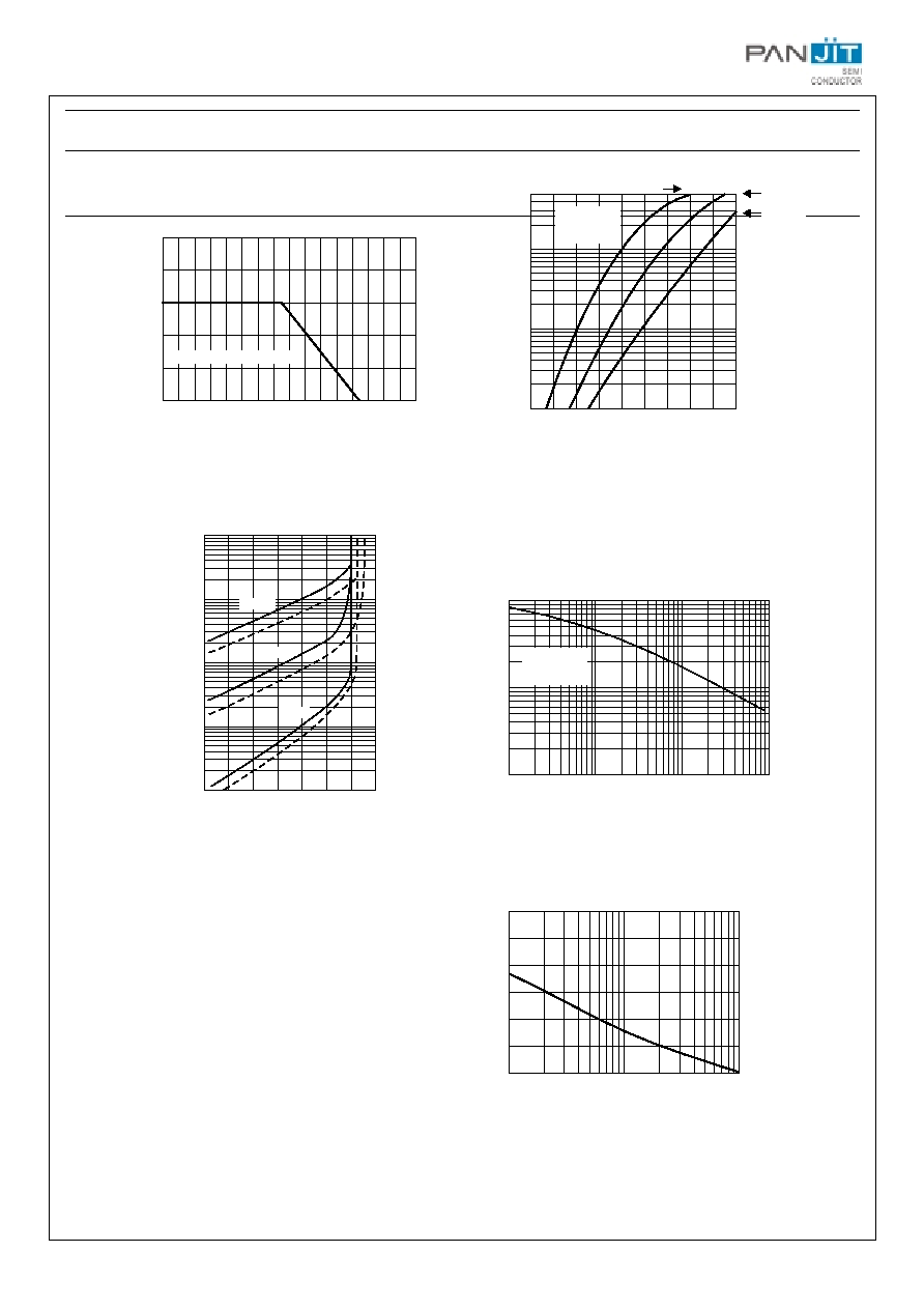
Fig.2- TYPICAL INSTANTANEOUS FORWARD
CHARACTERISTIC
INSTANTANEOUS FORWARD VOLTAGE, VOLTS
A
VERAGE
F
OR
W
A
RD
RECITIFIED
CURRENT
AMPERES
Fig.1- FORWARD CURRENT DERATING CURVE
CASE TEMPERATURE, C
O
.4
.5
.6
.7
.8
.9 1.0 1.1
50
0.1
Fig.3- TYPICAL REVERSE CHARACTERISTIC
INST
ANT
ANEOUS
REVERSE
CURRENT
,
M
ILAMPERES
20 40 60 80 100 120 140
10
1.0
0.10
0.01
.001
PEAK
FOR
W
ARD
SURGE
C
URRENT
,
AMPERES
NUMBER OF CYCLE AT 60HZ
1000
10
0.1
1.0
10
100
CAP
ACIT
ANCE,
pF
Fig.4- TYPICAL JUNCTION CAPACITANCE
REVERSE VOLTAGE, VOLTS
1
10
100
120
100
80
60
40
20
0
10.0
8.0
4.0
0
10
1.0
.3
.2
100
Fig.5- MAXIMUM NON-REPETITIVE PEAK
FORWARD SURGE CURRENT
RESISTIVE OR INDUCTIVE LOAD
T = 25 C
f = 1.0mHz
Vsig = 50mVp-p
J
O
T = 100 C
J
O
T = 75 C
J
O
T = 25 C
J
O
T = 25 C
f = 1.0mHz
Vsig = 50mVp-p
J
O
2.0
6.0
0
20
40
60
80
100
120
140
160
50 - 60 V
20 - 40 V
80 - 100 V