1
PS8431 09/24/99
12345678901234567890123456789012123456789012345678901234567890121234567890123456789012345678901212345678901234567890123456789012123456789012
12345678901234567890123456789012123456789012345678901234567890121234567890123456789012345678901212345678901234567890123456789012123456789012
12345678901234567890123456789012123456789012345678901234567890121234567890123456789012345678901212345678901234567890123456789012123456789012
Product Description
Pericom Semiconductors GTLP series of logic circuits are produced
using the Companys advanced 0.5 micron CMOS technology,
achieving industry leading performance.
The GTLP16612A 18-bit universal transceiver provides TTL to GTLP
signal level translation. The device is designed to provide high-
speed interface between cards operating at TTL logic levels and a
back plane operating at GTLP logic levels. High-speed back plane
operation is a direct result of GTLPs reduced output swing (<1V),
reduced input threshold levels, and output edge-rate control which
minimizes signal settling times. Its function is similar to BTL or GTL
but with modified driver output levels and receiver threshold. GTLP
output low voltage is typically less than 0.5V, the output high is 1.5V,
and the receiver threshold is 1.0V.
Features
Bidirectional interface between GTLP and TTL
logic levels
Designed with Edge Rate Control Circuit to
reduce output noise
V
REF
pin provides external supply reference voltage
for receiver threshold
5V tolerant inputs and outputs on A-Port
Increased B-Port Drive, 50mA
Bus-Hold data inputs on A-Port to eliminate the need for
pull-up resistors for unused inputs
Power up/down high impedance
TTL compatible Driver and Control inputs
A-Port Balanced Drive: 32mA/+32mA
Flow-through architecture
Open drain on GTLP to support wired-or connection
Package:
56-pin 240 Mil Wide Plastic TSSOP (A)
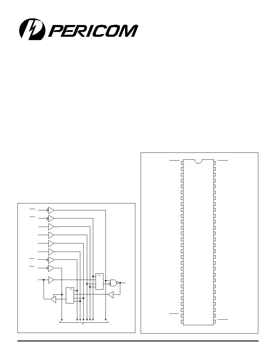
Pin Configuration
Logic Block Diagram
GTLP16612A
CMOS 18-Bit TTL/GTLP Universal Bus Transceiver
CLK
CI
1D
CE
GTLP
OEAB
CEAB
LEAB
LEBA
CEBA
OEBA
A1 3
CLKAB
CLKBA
1
56
2
28
29
27
54
B1
55
30
V
CLK
CI
1D
CE
V
1 of 18 Channels
1 of 18 Channels
OEAB
LEAB
CEAB
CLKAB
1
2
A1
A2
A3
A4
A6
A5
A7
A9
A8
A10
A12
A11
A13
A15
A14
A17
A18
B18
B17
B16
B15
B14
B13
B12
B11
B10
B9
B8
B7
B6
B5
B4
B3
B2
A16
3
GND
4
5
6
7
V
CC
(3.3V)
8
9
10
GND
11
12
13
14
15
16
17
GND
18
19
20
21
V
CC
(3.3V)
22
23
24
56
55
B
1
54
GND
53
52
51
V
CCQ
(5.0V)
50
49
48
47
GND
46
45
44
43
42
41
40
GND
39
38
37
36
V
REF
35
34
33
GND
25
26
27
LEBA
OEBA
28
GND
32
31
CLKBA
30
CEBA
29
56-Pin
A,V

2
PS8431 09/24/99
GTLP16612A
CMOS 18-Bit TTL/GTLP
Universal Bus Transceiver
12345678901234567890123456789012123456789012345678901234567890121234567890123456789012345678901212345678901234567890123456789012123456789012
12345678901234567890123456789012123456789012345678901234567890121234567890123456789012345678901212345678901234567890123456789012123456789012
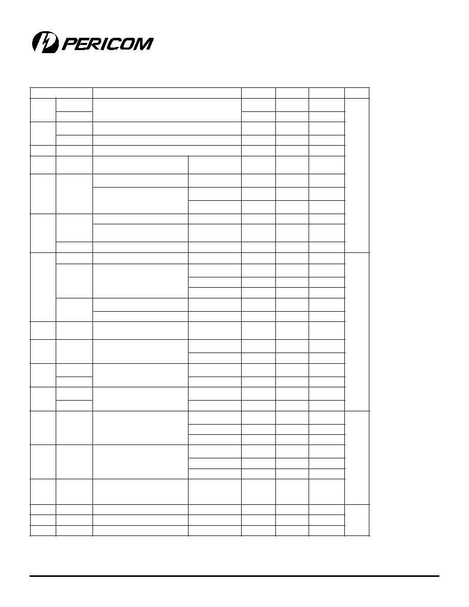
Notes:
1. A-to-B data flow is shown. B-to-A data flow is similar but uses OEBA,
LEBA, CLKBA, and CEBA.
2. Output level before indicated steady-state input conditions were estab-
lished, provided CLKAB was HIGH before LEAB went LOW.
3. Output level before indicated steady-state input conditions were estab-
lished.
s
t
u
p
n
I
B
t
u
p
t
u
O
e
d
o
M
B
A
E
C
B
A
E
O
B
A
E
L
B
A
K
L
C
A
X
H
X
X
X
Z
d
e
h
c
t
a
L
e
g
a
r
o
t
S
a
t
a
D
A
f
o
L
L
L
H
X
B
0 )
2
(
L
L
L
L
X
B
0 )
3
(
X
L
H
X
L
L
t
n
e
r
a
p
s
n
a
r
T
X
L
H
X
H
H
L
L
L
L
L
e
g
a
r
o
t
S
d
e
k
c
o
l
C
a
t
a
D
A
f
o
L
L
L
H
H
H
L
L
X
X
B
0 )
3
(
ti
b
i
h
n
I
k
c
o
l
C
Pin Descriptions
Truth Table
(1)
s
e
m
a
N
n
i
P
n
o
it
p
i
r
c
s
e
D
B
A
E
O
)
W
O
L
e
v
it
c
A
(
el
b
a
n
E
t
u
p
t
u
O
B
-
o
t
-
A
A
B
E
O
)
W
O
L
e
v
it
c
A
(
el
b
a
n
E
t
u
p
t
u
O
A
-
o
t
-
B
B
A
E
C
)
W
O
L
e
v
it
c
A
(
el
b
a
n
E
k
c
o
l
C
B
-
o
t
-
A
A
B
E
C
)
W
O
L
e
v
it
c
A
(
el
b
a
n
E
k
c
o
l
C
A
-
o
t
-
B
B
A
E
L
)
H
G
I
H
t
n
e
r
a
p
s
n
a
r
T
(
el
b
a
n
E
h
c
t
a
L
B
-
o
t
-
A
A
B
E
L
)
H
G
I
H
t
n
e
r
a
p
s
n
a
r
T
(
el
b
a
n
E
h
c
t
a
L
A
-
o
t
-
B
B
A
K
L
C
e
sl
u
P
k
c
o
l
C
B
-
o
t
-
A
A
B
K
L
C
e
sl
u
P
k
c
o
l
C
A
-
o
t
-
B
F
E
R
V
e
g
a
tl
o
V
e
c
n
e
r
e
f
e
R
t
u
p
n
I
P
L
T
G
8
1
A
-
1
A
r
o
st
u
p
n
I
a
t
a
D
L
T
T
B
-
o
t
-
A
st
u
p
t
u
O
e
t
a
t
S
-
3
A
-
o
t
-
B
8
1
B
-
1
B
r
o
st
u
p
n
I
a
t
a
D
P
L
T
G
A
-
o
t
-
B
st
u
p
t
u
O
n
i
a
r
D
n
e
p
O
B
-
o
t
-
A
Functional Description
The PI74GTLP16612A combines a universal transceiver function with a TTL to GTLP translation. The A-Port and control pins operate
at LVTTL or 5V TTL levels while the B-Port operates at GTLP levels. The transceiver logic includes D-type latches and D-type flip-flops
to allow data flow in transparent, latched, and clock mode. The functional operation is described below:

3
PS8431 09/24/99
GTLP16612A
CMOS 18-Bit TTL/GTLP
Universal Bus Transceiver
123456789012345678901234567890121234567890123456789012345678901212345678901234567890123456789012123456789012345678901234567890121234567890123
123456789012345678901234567890121234567890123456789012345678901212345678901234567890123456789012123456789012345678901234567890121234567890123
Storage Temperature (T
STG
) ............................................... 65�C to +150�C
Supply Voltage (V
CC
, V
CCQ
) ................................................... 0.5V to +7.0V
DC Input Voltage (V
I
) ........................................................... 0.5V to +7.0V
DC Output Voltage (V
O
)
Outputs 3-State .................................................................. 0.5V to +7.0V
Outputs Active
(5)
........................................................ 0.5V to V
CC
+0.5V
DC Output Current into A-Port I
OH
/I
OL
............................... 64mA/+64mA
DC Output Sink Current into B-Port in LOW State I
OL
......................100mA
DC Input Diode Current (I
IK
)
V
I
< 0V ............................................................................................ 50mA
DC Output Diode Current (I
OK
)
V
O
< 0V ........................................................................................... 50mA
V
O
> V
CC
.......................................................................................... +50mA
ESD Performance .............................................................................. >2000V
Notes:
4. The Absolute Maximum Ratings are those values beyond which the safety
of the device cannot be guaranteed. The device should not be operated at
these limits. The parametric values defined in the Electrical Characteristic
tables are not guaranteed at the absolute maximum rating. The Recommended
Operating Conditions table will define the conditions for actual device
operation.
5. I
O
Absolute Maximum Rating must be observed
6. Unused inputs must be held HIGH or LOW.
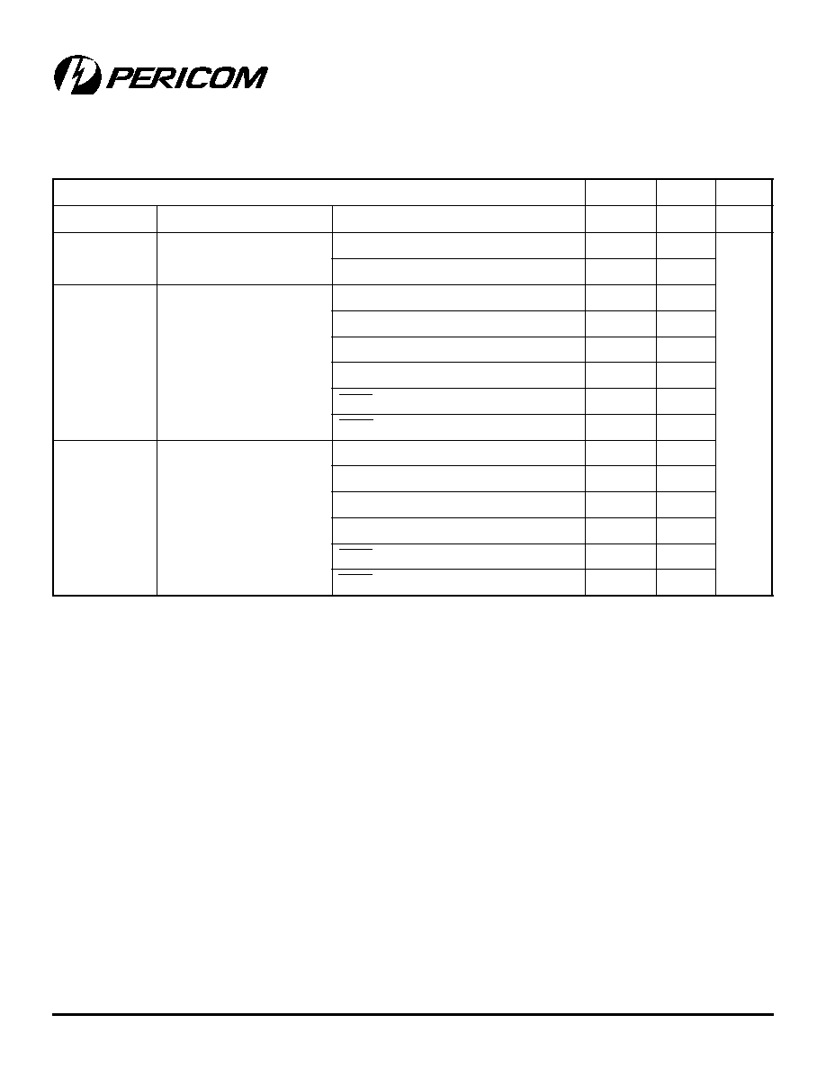
Recommended Operating Condition
(6)
Absolute Maximum Ratings
(4)
(Above which the useful life may be impaired. For user guidelines, not tested.)
Supply Voltage (V
CC
)
V
CC
....................................................................................... 3.15V to 3.45V
V
CCQ
..................................................................................... 4.75V to 5.25V
Bus Termination Voltage (V
TT
) .............................................. 1.35V to 1.65V
Input Voltage (V
I
) on A-Port and Control Pins ........................ 0.0V to 5.5V
HIGH Level Output Current (I
OH
)
A-Port ............................................................................................ 32mA
LOW Level Output Current (I
OL
)
A-Port ............................................................................................ +32mA
B-Port ............................................................................................. +50mA
Operating Temperature (T
A
) ................................................ 40�C to +85�C
4
PS8431 09/24/99
GTLP16612A
CMOS 18-Bit TTL/GTLP
Universal Bus Transceiver
12345678901234567890123456789012123456789012345678901234567890121234567890123456789012345678901212345678901234567890123456789012123456789012
12345678901234567890123456789012123456789012345678901234567890121234567890123456789012345678901212345678901234567890123456789012123456789012
Notes:
7. All typical values are at V
CC
= 3.3V, V
CCQ
= 5.0V, and T
A
= 25�C
8. For conditions shown as Max. or Min., use the appropriate value specified under recommended operating conditions.
9. This is the increase in supply current for each input that is at the specified TTL voltage level rather than V
CC
or GND.
DC Electrical Characteristics
(Over the Operating Free-Air Temperature Range, V
REF
= 1.0 (Unless otherwise noted)
l
o
b
m
y
S
s
n
o
it
i
d
n
o
C
t
s
e
T
.
n
i
M
p
y
T
)
7
(
.
x
a
M
s
ti
n
U
V
H
I
tr
o
P
-
B
V
F
E
R
1
.
0
+
V
T
T
V
s
r
e
h
t
O
0
.
2
V
L
I
tr
o
P
-
B
0
.
0
V
F
E
R
1
.
0
s
r
e
h
t
O
8
.
0
V
F
E
R
0
.
1
V
K
I
V
C
C
,
V
5
1
.
3
=
V
Q
C
C
V
5
7
.
4
=
I
I
A
m
8
1
=
2
.
1
V
H
O
tr
o
P
-
A
V
C
C
V
,
Q
C
C
x
a
M
o
t
.
n
i
M
=
)
8
(
I
H
O
0
0
1
=
�
A
V
C
C
2
.
0
V
C
C
V
5
1
.
3
=
V
Q
C
C
V
5
7
.
4
=
I
H
O
A
m
8
=
4
.
2
I
H
O
A
m
2
3
=
0
.
2
V
L
O
tr
o
P
-
A
V
C
C
V
,
Q
C
C
x
a
M
o
t
.
n
i
M
=
)
8
(
I
L
O
0
0
1
=
�
A
2
.
0
V
C
C
V
5
1
.
3
=
V
Q
C
C
V
5
7
.
4
=
I
L
O
A
m
2
3
=
5
.
0
tr
o
P
-
B
V
C
C
V
,
V
5
1
.
3
=
Q
C
C
V
5
7
.
4
=
I
L
O
A
m
0
5
=
5
6
.
0
I
I
s
n
i
P
l
o
rt
n
o
C
V
C
C
V
,
Q
C
C
x
a
M
r
o
0
=
V
I
V
0
r
o
V
5
.
5
=
0
1
�
�
A
tr
o
P
-
A
V
C
C
V
5
4
.
3
=
V
Q
C
C
V
5
2
.
5
=
V
I
V
5
.
5
=
0
2
V
I
V
=
C
C
1
V
I
0
=
0
3
tr
o
P
-
B
V
C
C
V
5
4
.
3
=
V
I
V
=
Q
C
C
5
V
Q
C
C
V
5
2
.
5
=
V
I
0
=
5
I
F
F
O
tr
o
P
-
A
V
C
C
V
=
Q
C
C
0
=
V
I
V
r
o
O
o
t
0
=
V
5
.
4
0
0
1
I
)
D
L
O
H
(I
tr
o
P
-
A
V
C
C
,
V
5
1
.
3
=
V
Q
C
C
V
5
7
.
4
=
V
I
V
8
.
0
=
5
7
V
I
V
0
.
2
=
0
2
I
H
Z
O
tr
o
P
-
A
V
C
C
,
V
5
4
.
3
=
V
Q
C
C
V
5
2
.
5
=
V
O
V
5
4
.
3
=
1
tr
o
P
-
B
V
O
V
5
.
1
=
5
I
L
Z
O
tr
o
P
-
A
V
C
C
V
5
4
.
3
=
V
Q
C
C
V
5
2
.
5
=
V
O
0
=
0
2
tr
o
P
-
B
V
O
V
5
6
.
0
=
0
1
I
Q
C
C
V
(
Q
C
C
)
B
r
o
A
st
r
o
P
V
C
C
,
V
5
4
.
3
=
V
Q
C
C
,
V
5
2
.
5
=
I
O
,
0
=
V
I
V
=
Q
C
C
D
N
G
r
o
H
G
I
H
st
u
p
t
u
O
0
3
0
4
A
m
W
O
L
st
u
p
t
u
O
0
3
0
4
d
el
b
a
si
D
st
u
p
t
u
O
0
3
0
4
I
C
C
V
(
C
C
)
B
r
o
A
st
r
o
P
V
C
C
,
V
5
4
.
3
=
V
Q
C
C
,
V
5
2
.
5
=
I
O
,
0
=
V
I
V
=
Q
C
C
D
N
G
r
o
H
G
I
H
st
u
p
t
u
O
0
1
W
O
L
st
u
p
t
u
O
0
1
d
el
b
a
si
D
st
u
p
t
u
O
0
1
C
C
)
9
(
d
n
a
tr
o
P
-
A
s
n
i
P
l
o
rt
n
o
C
V
C
C
,
V
5
4
.
3
=
V
Q
C
C
,
V
5
2
.
5
=
V
t
a
st
u
p
n
I
l
o
rt
n
o
C
r
o
A
C
C
D
N
G
r
o
V
7
.
2
t
a
t
u
p
n
I
e
n
O
0
1
C
N
I
s
n
i
P
l
o
rt
n
o
C
V
I
V
=
Q
C
C
0
r
o
8
F
p
C
O
/I
tr
o
P
-
A
V
I
V
=
Q
C
C
0
r
o
9
C
O
/I
tr
o
P
-
B
V
I
V
=
Q
C
C
0
r
o
8
5
PS8431 09/24/99
GTLP16612A
CMOS 18-Bit TTL/GTLP
Universal Bus Transceiver
123456789012345678901234567890121234567890123456789012345678901212345678901234567890123456789012123456789012345678901234567890121234567890123
123456789012345678901234567890121234567890123456789012345678901212345678901234567890123456789012123456789012345678901234567890121234567890123
l
o
b
m
y
S
.
n
i
M
.
x
a
M
s
ti
n
U
f
K
C
O
L
C
y
c
n
e
u
q
e
r
F
k
c
o
l
C
x
a
M
5
7
1
z
H
M
t
W
n
o
it
a
r
u
D
e
sl
u
P
H
G
I
H
A
B
E
L
r
o
B
A
E
L
0
.
3
s
n
W
O
L
r
o
H
G
I
H
A
B
K
L
C
r
o
B
A
K
L
C
2
.
3
t
S
e
m
i
T
p
u
t
e
S
B
A
K
L
C
e
r
o
f
e
b
A
5
.
0
A
B
K
L
C
e
r
o
f
e
b
B
1
.
3
B
A
E
L
e
r
o
f
e
b
A
3
.
1
A
B
E
L
e
r
o
f
e
b
B
7
.
3
B
A
K
L
C
e
r
o
f
e
b
B
A
E
C
4
.
0
A
B
K
L
C
e
r
o
f
e
b
A
B
E
C
0
.
1
t
H
e
m
i
T
d
l
o
H
B
A
K
L
C
r
e
tf
a
A
5
.
1
A
B
K
L
C
r
e
tf
a
B
0
.
0
B
A
E
L
r
e
tf
a
A
5
.
0
A
B
E
L
r
e
tf
a
B
0
.
0
B
A
K
L
C
r
e
tf
a
B
A
E
C
5
.
1
A
B
K
L
C
r
e
tf
a
A
B
E
C
7
.
1
AC Operating Requirements
(Over recommended ranges of supply voltage and operating free-air temperature, V
REF
= 1.0 (Unless otherwise noted)