1
PS8401C 09/24/04
NC
1
2
3
4
5
6
7
8
9
GND
10
11
12
13
14
15
16
17
18
19
20
GND
BE1
40
39
38
37
36
35
V
CC
34
33
32
31
30
29
28
27
26
25
24
23
22
B
15
21
A
0
A
1
A
2
A
3
A
4
A
5
A
6
A
7
NC
A
8
A
9
A
10
A
11
A
12
A
13
A
14
A
15
B
14
B
13
B
12
B
11
B
10
B
9
B
8
BE2
V
CC
B
0
B
1
B
2
B
3
B
4
B
5
B
6
B
7
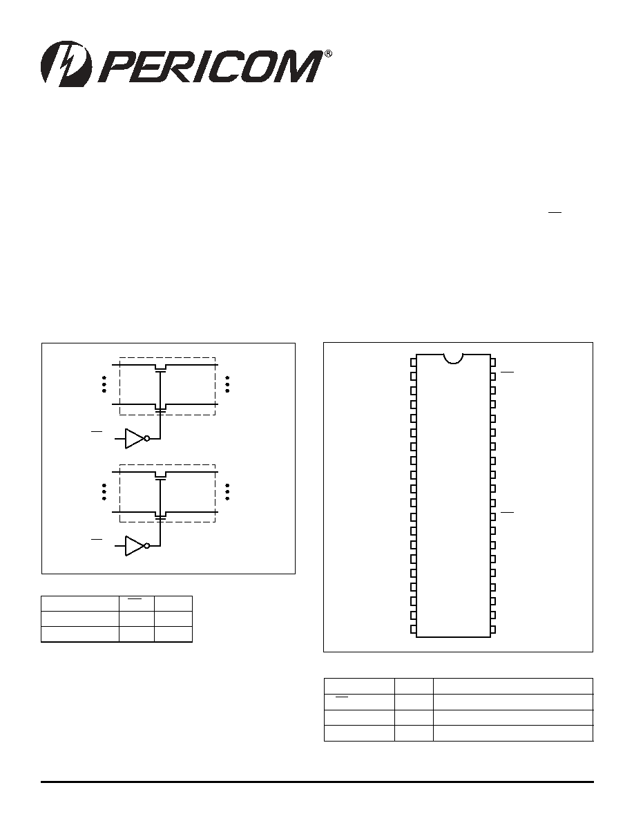
Description
Pericom Semiconductor's PI3C32X245 is a 2.5V or 3.3V 16-bit, 2-port
bus switch designed with a low On-Resistance (5-ohm) allowing
inputs to be connected directly to outputs. The bus switch creates
no additional propagational delay or additional ground bounce
noise. The switches are turned ON by the Bus Enable (BE
N
) input
signal. It is very useful in switching signals that have high bandwidth
(>400 MHz).
Function
BE
N
A0≠15
Disconnect
H
Hi-Z
Connect
L
B0≠15
Truth Table
(1)
Note:
1. H
= High Voltage Level
L
= Low Voltage Level
Hi-Z = High Impedance
Block Diagram
Pin Description
Pin Name
I/O
Description
BE
N
I
Bus Enable Input (Active LOW)
A0≠A15
I/O
Bus A
B0≠B15
I/O
Bus A
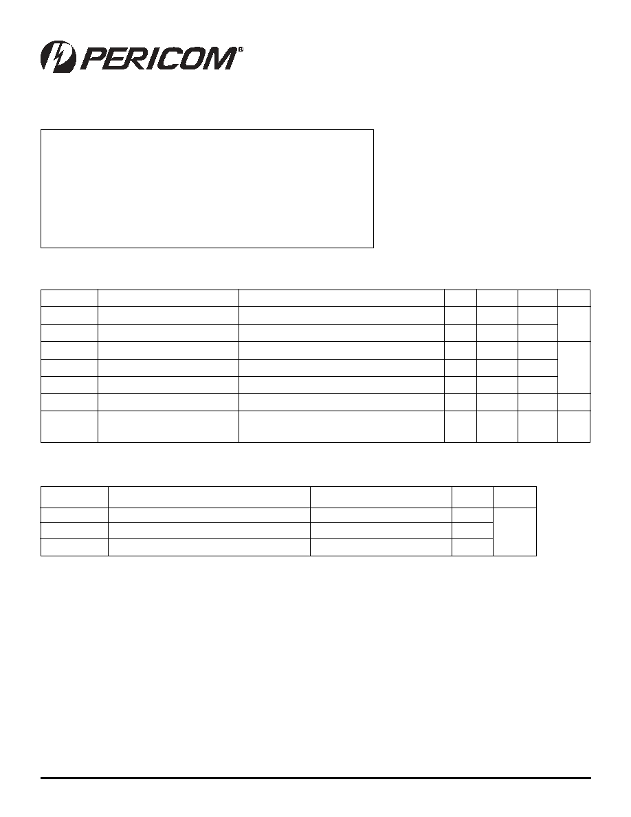
Pin Configuration
Features
∑ Near-Zero propagation delay
∑ 5-ohm switches connect inputs to outputs
∑ Permits Hot Insertion
∑ 5V I/O Tolerant
∑ 2.5V Supply Voltage Operation
∑ Rail-to-Rail 3.3Vor 2.5V Switching
∑ High Bandwidth Operation (>400 MHz)
∑ Packaging (Pb-free & Green available)
≠ 40-pin, 150-mil-wide plastic BQSOP (B)
40-Pin
B
A
7
A
0
B
7
B
0
BE
1
A
15
A
8
B
15
B
8
BE
2
PI3C32X245
2.5V/3.3V, High Bandwidth, Hot Insertion
16-Bit, 2-Port, Bus Switch
12345678901234567890123456789012123456789012345678901234567890121234567890123456789012345678901212345678901234567890123456789012123456789012
12345678901234567890123456789012123456789012345678901234567890121234567890123456789012345678901212345678901234567890123456789012123456789012
2
PS8401C 09/24/04
12345678901234567890123456789012123456789012345678901234567890121234567890123456789012345678901212345678901234567890123456789012123456789012
12345678901234567890123456789012123456789012345678901234567890121234567890123456789012345678901212345678901234567890123456789012123456789012
12345678901234567890123456789012123456789012345678901234567890121234567890123456789012345678901212345678901234567890123456789012123456789012
12345678901234567890123456789012123456789012345678901234567890121234567890123456789012345678901212345678901234567890123456789012123456789012
PI3C32X245
2.5V/3.3V, High Bandwidth,
Hot Insertion, 16-Bit, 2-Port, Bus Switch
Storage Temperature.............................................................. ≠65∞C to +150∞C
Ambient Temperature with Power Applied ................................ ≠40∞C to +85∞C
Supply Voltage to Ground Potential (Inputs & V
CC
Only) ......... ≠0.5V to +4.6V
Supply Voltage to Ground Potential (Outputs & D/O Only) ....... ≠0.5V to +4.6V
DC Input Voltage ........................................................................ ≠0.5V to +5.5V
DC Output Current .................................................................................. 120mA
Power Dissipation ......................................................................................0.5W
Note:
Stresses greater than those listed under MAXIMUM
RATINGS may cause permanent damage to the de-
vice. This is a stress rating only and functional
operation of the device at these or any other condi-
tions above those indicated in the operational sec-
tions of this specification is not implied. Exposure
to absolute maximum rating conditions for extended
periods may affect reliability.
Maximum Ratings
(Above which the useful life may be impaired. For user guidelines, not tested.)
Parameters
(5)
Description
Test Conditions
Typ.
Units
C
IN
Input Capacitance
V
IN
= 0V
3.5
C
OFF
A/B Capacitance, Switch Off
V
IN
= 0V
5.0
pF
C
ON
A/B Capacitance, Switch On
V
IN
= 0V
10.0
Notes:
1. For Max. or Min. conditions, use appropriate value specified under Electrical Characteristics for the applicable
device type.
2. Typical values are at V
CC
= 3.3V, T
A
= 25∞C ambient and maximum loading.
3. Not more than one output should be shorted at one time. Duration of the test should not exceed one second.
4. Measured by the voltage drop between A and B pin at indicated current through the switch. ON resistance is
determined by the lower of the voltages on the two (A,B) pins.
5. This parameter is determined by device characterization but is not production tested.
V
Capacitance
(T
A
= 25∞C, f = 1 MHz)
DC Electrical Characteristics
(Over Operating Range, T
A
= ≠40∞C to +85∞C, V
CC
= 3.3V ±10%)
Parameters Description
Test Conditions
(1)
Min.
Typ.
(2)
Max.
Units
V
IH
Input HIGH Voltage
Guaranteed Logic HIGH Level
2.0
V
IL
Input LOW Voltage
Guaranteed Logic LOW Level
≠0.5
0.8
I
IH
Input HIGH Current
V
CC
= Max., V
IN
= V
CC
±1
I
IL
Input LOW Current
V
CC
= Max., V
IN
= GND
±1
µA
I
OZH
High Impedance Output Current 0
A, B
V
CC
±1
V
IK
Clamp Diode Voltage
V
CC
= Min., I
IN
= ≠18mA
≠0.73
≠1.2
V
R
ON
Switch On Resistance
(4)
V
CC
= Min., V
IN
= 0.0V, I
ON
= 48mA
5
7
V
CC
= Min., V
IN
= 2.4V, I
ON
= 15mA
8
15
PI3C32X245
2.5V/3.3V, High Bandwidth,
Hot Insertion, 16-Bit, 2-Port, Bus Switch
3
PS8401C 09/24/04
12345678901234567890123456789012123456789012345678901234567890121234567890123456789012345678901212345678901234567890123456789012123456789012
12345678901234567890123456789012123456789012345678901234567890121234567890123456789012345678901212345678901234567890123456789012123456789012
12345678901234567890123456789012123456789012345678901234567890121234567890123456789012345678901212345678901234567890123456789012123456789012
12345678901234567890123456789012123456789012345678901234567890121234567890123456789012345678901212345678901234567890123456789012123456789012
s
r
e
t
e
m
a
r
a
P
n
o
i
t
p
i
r
c
s
e
D
s
n
o
i
t
i
d
n
o
C
5
4
2
X
2
3
C
3
1
P
s
t
i
n
U
.
m
o
C
.
n
i
M
.
x
a
M
t
H
L
P
t
L
H
P
y
a
l
e
D
n
o
it
a
g
a
p
o
r
P
)
3
,
2
(
x
B
o
t
x
A
C
L
F
p
0
5
=
R
L
m
h
o
0
0
5
=
5
2
.
0
s
n
t
H
Z
P
t
L
Z
P
e
m
i
T
e
l
b
a
n
E
s
u
B
x
B
r
o
x
A
o
t
E
B
C
L
F
p
0
5
=
R
L
m
h
o
0
0
5
=
m
h
o
0
0
5
=
R
5
.
1
8
.
9
t
Z
H
P
t
Z
L
P
e
m
i
T
e
l
b
a
si
D
s
u
B
x
B
r
o
x
A
o
t
E
B
5
.
1
3
.
8
Notes:
1. For Max. or Min. conditions, use appropriate value specified under Electrical Characteristics for the applicable device.
2. Typical values are at V
CC
= 3.3V, +25∞C ambient.
3. Per driven input (control input only); A and B pins do not contribute to
I
CC
.
Switching Characteristics over 3.3V Operating Range
mA
Power Supply Characteristics
Parameters Description
Test Conditions
(1)
Min.
Typ.
(2)
Max.
Units
I
CC
Quiescent Power
V
CC
= Max.
V
IN
= GND or V
CC
0.5
1.0
Supply Current
I
CC
Supply Current per
V
CC
= Max.
V
IN
= 3.0V
(3)
2.5
Input HIGH
Switching Characteristics over 2.5V Operating Range
s
r
e
t
e
m
a
r
a
P
n
o
i
t
p
i
r
c
s
e
D
s
n
o
i
t
i
d
n
o
C
5
4
2
X
2
3
C
3
1
P
s
t
i
n
U
.
m
o
C
.
n
i
M
.
x
a
M
t
H
L
P
t
L
H
P
y
a
l
e
D
n
o
it
a
g
a
p
o
r
P
)
3
,
2
(
x
B
o
t
x
A
C
L
F
p
0
5
=
R
L
m
h
o
0
0
5
=
5
2
.
0
s
n
t
H
Z
P
t
L
Z
P
e
m
i
T
e
l
b
a
n
E
s
u
B
x
B
r
o
x
A
o
t
E
B
C
L
F
p
0
5
=
R
L
m
h
o
0
0
5
=
m
h
o
0
0
5
=
R
5
.
1
8
.
9
t
Z
H
P
t
Z
L
P
e
m
i
T
e
l
b
a
si
D
s
u
B
x
B
r
o
x
A
o
t
E
B
5
.
1
3
.
8
Notes:
1. See test circuit and waveforms.
2. This parameter is guaranteed but not tested on Propagation Delays.
3. The bus switch contributes no propagational delay other than the RC delay of the ON resistance of the switch and the load
capacitance. The time constant for the switch alone is of the order of 0.25ns for 50pF load. Since this time constant is much smaller
than the rise/fall times of typical driving signals, it adds very little propagational delay to the system. Propagational delay of the
bus switch when used in a system is determined by the driving circuit on the driving side of the switch and its interaction with the
load on the driven side.
PI3C32X245
PI3C32X245
6.5
5.5
4
PS8401C 09/24/04
12345678901234567890123456789012123456789012345678901234567890121234567890123456789012345678901212345678901234567890123456789012123456789012
12345678901234567890123456789012123456789012345678901234567890121234567890123456789012345678901212345678901234567890123456789012123456789012
12345678901234567890123456789012123456789012345678901234567890121234567890123456789012345678901212345678901234567890123456789012123456789012
12345678901234567890123456789012123456789012345678901234567890121234567890123456789012345678901212345678901234567890123456789012123456789012
PI3C32X245
2.5V/3.3V, High Bandwidth,
Hot Insertion, 16-Bit, 2-Port, Bus Switch
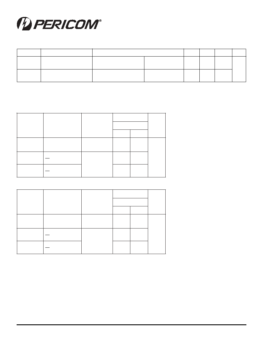
4.0
2.0
0.0
0.0
1.0
2.0
3.0
4.0
5.0
V
OUT
, (V)
VIN, (V)
VCC =
3.3V
3.1V
2.9V
2.7V
2.5V
2.3V
3.6V
3.8V
3.4V
3.2V
3.0V
2.8V
Output Voltage vs. Input Voltage over Various Supply Voltages
Output Voltage vs. Input Voltage over Various Supply Voltages
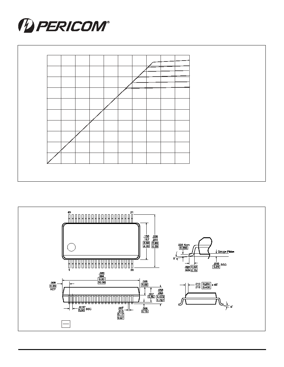
Packaging Mechanical: 40-pin BQSOP (B)
X.XX
X.XX
DENOTES DIMENSION IN MILLIMETERS

PI3C32X245
2.5V/3.3V, High Bandwidth,
Hot Insertion, 16-Bit, 2-Port, Bus Switch
5
PS8401C 09/24/04
12345678901234567890123456789012123456789012345678901234567890121234567890123456789012345678901212345678901234567890123456789012123456789012
12345678901234567890123456789012123456789012345678901234567890121234567890123456789012345678901212345678901234567890123456789012123456789012
12345678901234567890123456789012123456789012345678901234567890121234567890123456789012345678901212345678901234567890123456789012123456789012
12345678901234567890123456789012123456789012345678901234567890121234567890123456789012345678901212345678901234567890123456789012123456789012
Notes:
1. Thermal characteristics can be found on the company web site at www.pericom.com/packaging/
Ordering Information
Ordering Code
Package Code
Package Type
PI3C32X245B
B
40-pin BQSOP
PI3C32X245BE
B
Pb-free & Green, 40-pin BQSOP
Pericom Semiconductor Corporation ∑ 1-800-435-2336 ∑ www.pericom.com