 | –≠–ª–µ–∫—Ç—Ä–æ–Ω–Ω—ã–π –∫–æ–º–ø–æ–Ω–µ–Ω—Ç: PI3L110QE | –°–∫–∞—á–∞—Ç—å:  PDF PDF  ZIP ZIP |

1
PS8690A 09/22/04
Features
∑ R
ON
is 4s typical
∑ Low crosstalk: ≠27dB @ 250MHz
∑ Near-Zero propagation delay: 250ps
∑ Switching speed: 9ns
∑ Channel On capacitance: 9pF (typical)
∑ V
CC
Operating Range: +3.0V to +3.6V
∑ ESD>2000V . . . Human Body Model
∑ >350 MHz bandwidth (or data frequency)
∑ Packaging (Pb-free & Green available)
16-pin 150 mil wide plastic QSOP (Q)
16-pin 173 mil wide plastic TSSOP(L)
Applications
∑ Dual Physical Layer Device sharing to one interface
connector
∑ Routes signals for 10/100 Mbit Ethernet
Description
Pericom Semiconductor's PI3L series of logic circuits are produced
using the Company's advanced sub-micron CMOS technology,
achieving industry leading performance.
The PI3L110 is a 8- to 4-bit multiplexer/demultiplexer LAN
Switch with Hi-Z outputs. Industry leading advantages include a
propagation delay of less than 250ps, resulting from its low channel
resistance and I/O capacitance. The device multiplexes differential
outputs from a Fast Ethernet transceiver (PHY) device to one of
two corresponding outputs. The switch is bidirectional and offers
little or no attenuation of the high-speed signals at the outputs. It
is designed for low bit-to-bit skew, high channel-to-channel noise
isolation and is compatible with various standards, such as 10/100
Base-T (Ethernet).
Generally, this part can be used to replace mechanical relays in
low-voltage LAN applications that interface a physical layer over
CAT 5 or CAT 6 unshielded twisted pair cable through an isolation
transformer.
Block Diagram
Pin Configuration
PI3L110
3.3V Quad, 2:1 Mux/DeMux
Fast Ethernet LAN Switch w/ Single Enable
V
CC
1
S
16
E
2
I
A
0
15
I
D
0
3
I
A
1
14
I
D
1
4
Y
A
13
Y
D
5
I
B
0
12
I
C
0
6
I
B
1
11
I
C
1
7
Y
B
10
Y
C
8
GND
9
E
I
A
0 I
A
1 I
B
0 I
B
1 I
C
0 I
C
1 I
D
0 I
D
1
S
Y
A
Y
B
Y
C
Y
D

2
PS8690A 09/22/04
PI3L110
3.3V Quad, 2:1 Mux/DeMux
Fast Ethernet LAN Switch w/ Single Enable
Pin Description
Pin Name
Description
I
A
N
-
I
D
N
Data Inputs
S
Select Inputs
E
Enable
YA-YD
Data Outputs
GND
Ground
V
CC
Power
Storage Temperature ......................................... ≠65∞C to +150∞C
Supply Voltage to Ground Potential .............≠0.5V to +4.0V
DC Input Voltage .................................................≠0.5V to +5.5V
DC Output Current............................................................ 120mA
Power Dissipation ................................................................ 0.5W
Note: Stresses greater than those listed under MAXIMUM RAT-
INGS may cause permanent damage to the device. This is a stress
rating only and functional operation of the device at these or any other
conditions above those indicated in the operational sections of this
specification is not implied. Exposure to absolute maximum rating
conditions for extended periods may affect reliability.
Maximum Ratings
(Above which useful life may be impaired. For user guidelines, not tested.)
Truth Table
(1)
E
S
YA
YB
YC
YD
Function
H
X
Hi-Z
Hi-Z
Hi-Z
Hi-Z
Disable
L
L
I
A
0
I
B
0
I
C
0
I
D
0
S = 0
L
H
I
A
1
I
B
1
I
C
1
I
D
1
S = 1
Note:
1. H = High Voltage Level
L = Low Voltage Level
DC Electrical Characteristics for 10/100 Base-T Ethernet Switching over Operating Range
(T
A
= ≠40∞C to +85∞C, V
CC
= 3.3V ±10%)
Paramenter
Description
Test Conditions
Min.
Typ.
(2)
Max. Units
V
IH
Input HIGH Voltage
Guaranteed HIGH level
2.0
≠
≠
V
V
IL
Input LOW Voltage
Guaranteed LOW level
≠0.5
≠
0.8
V
IK
Clamp Diode Voltage
V
CC
= Max., I
IN
= ≠18mA
≠
≠0.7
≠1.2
I
IH
Input HIGH Current
V
CC
= Max., V
IN
= V
CC
≠
≠
±5
µA
I
IL
Input LOW Current
V
CC
= Max., V
IN
= GND
≠
≠
±5
R
ON
Switch On-Resistance
(3)
V
CC
= Min., 1.25V V
IN
V
CC
,
I
IN
= ≠10mA to ≠30mA
≠
4.0
8.0
R
FLAT(ON)
On-Resistance Flatness
(4)
V
CC
= Min., V
IN
@ 1.25V and V
CC,
I
IN
= ≠10mA to ≠30mA
≠
1
≠
R
ON
On-Resistance match from
center ports to any other port
(4)
V
CC
= Min., 1.25V V
IN
V
CC,
I
IN
= ≠10mA to ≠30mA
≠
0.9
2.0
3
PS8690A 09/22/04
PI3L110
3.3V Quad, 2:1 Mux/DeMux
Fast Ethernet LAN Switch w/ Single Enable
Characteristics
Paramenter
Description
Test Conditions
Min.
Typ.
(2)
Max.
Units
t
PD
Propagation Delay
(2,3)
≠
0.25
ns
t
PZH
, t
PZL
Line Enable Time - S or E to Y
N
, I
N
0.5
≠
15
t
PHZ
, t
PLZ
Line Disable Time - S to E to Y
N
, I
N
0.5
≠
9
t
SK(p)
Skew between opposite transitions of the
same output (t
PHL
- t
PLH
)
(2)
≠
0.1
0.2
Power Supply Characteristics
Notes:
1. For max. or min. conditions, use appropriate value specified under Electrical Characteristics for the applicable device type.
2. Typical values are at V
CC
= 3.3V, T
A
= 25∞C ambient and maximum loading.
3. Per TTL driven input (control inputs only); A and B pins do not contribute to I
CC
.
Notes:
1. For max. or min. conditions, use appropriate value specified under Electrical Characteristics for the applicable device type.
2. Typical values are at V
CC
= 3.3V, T
A
= 25∞C ambient and maximum loading.
3. Measured by the voltage drop between I
N
and Y
N
pins at indicated current through the switch. On-Resistance is determined by the lower of the
voltages on the two (I
N
& Y
N
) pins.
4. This parameter is determined by device characterization but is not production tested.
Notes:
1. For max. or min. conditions, use appropriate value specified under Electrical Characteristics for the applicable device type.
2. Guaranteed by design.
3. The bus switch contributes no propagational delay other than the RC delay of the On-Resistance of the switch and the load capacitance. The
time constant for the switch alone is of the order of 0.25ns for 10pF load. Since this time constant is much smaller than the rise/fall times of
typical driving signals, it adds very little propagational delay to the system. Propagational delay of the bus switch when used in a system is
determined by the driving circuit on the driving side of the switch and its interactions with the load on the driven side.
Capacitance
(T
A
= 25∞C, f = 1MHz)
Parameters
(4)
Description
Test Conditions
Typ.
Max.
Units
C
IN
Input Capacitance
V
IN
= 0V
2
3
pF
C
OFF(In)
Port I
N
Capacitance, Switch OFF
4
6
C
ON
Y
N
/I
N
Capacitance, Switch ON
9
10
Parameters
Description
Test Conditions
(1)
Min.
Typ.
(2)
Max.
Units
I
CC
Quiescent Power Supply Current
V
CC
= Max., V
IN
= GND or V
CC
--
--
800
µ
Dynamic Electrical Characteristics Over the Operating Range
(T
A
= ≠40∞C to +85∞C, V
CC
= 3.3V ±10%, GND = 0V)
Parameter
Description
Test Conditions
Min.
Typ.
(2)
Max.
Units
X
TALK
Crosstalk
R
L
= 50, f = 250MHz
--
-40
--
dB
O
IRR
OFF Isolation
--
≠30
--
BW
Bandwidth ≠3dB
R
L
= 50
--
350
--
MHz
4
PS8690A 09/22/04
PI3L110
3.3V Quad, 2:1 Mux/DeMux
Fast Ethernet LAN Switch w/ Single Enable
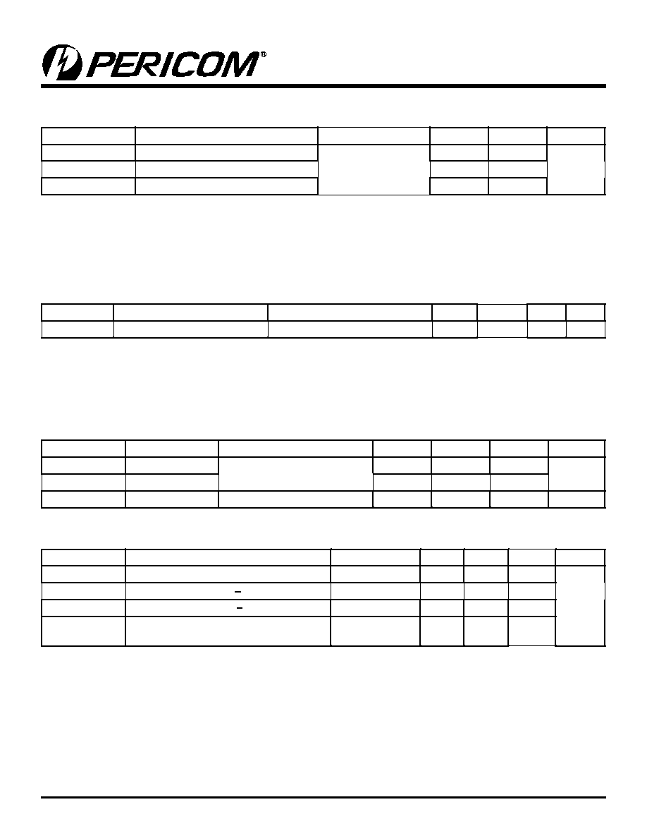
Test Circuit for Electrical Characteristics
(1)
Notes:
1. C
L
= Load capacitance: includes jig and probe capacitance.
2. R
T
= Termination resistance: should be equal to Z
OUT
of the Pulse Generator
3. Waveform 1 is for an output with internal conditions such that the output is low except when disabled by the output control.
Waveform 2 is for an output with internal conditions such that the output is high except when disabled by the output control.
4. All input impulses are supplied by generators having the following characteristics: PRR MHz, Z
O
= 50, t
R
2.5ns, t
F
2.5ns.
5. The outputs are measured one at a time with one transition per measurement.
Test Circuit for Dynamic Electrical Characteristics
R
T
10pF
C
L
V
CC
V
IN
V
OUT
200-ohm
200-ohm
6.0V
Pulse
Generator
D.U.T
V
CC
D.U.T
T1
R1
S1
HP11667A
50-ohm
10pF
HP4195A
Switch Positions
Test
Switch
t
PLZ
, t
PZL
6.0V
t
PHZ
, t
PZH
GND
Prop Delay
Open
5
PS8690A 09/22/04
PI3L110
3.3V Quad, 2:1 Mux/DeMux
Fast Ethernet LAN Switch w/ Single Enable
Switching Waveforms
Pulse Skew - t
SK(p)
Voltage Waveforms Enable and Disable Times
Applications Information
Logic Inputs
The logic control inputs can be driven up to +3.6V regardless of the supply voltage. For example, given a +3.3V supply, the output
enables or select pins may be driven low to 0V and high to 3.6V. Driving IN Rail-to-RailÆ minimizes power consumption.
Power-Supply Sequencing
Proper power-supply sequencing is advised for all CMOS devices. It is recommended to always apply V
CC
before applying signals to
the input/output or control pins.
Rail-to-Rail is a registered trademark of Nippon Motorola, Ltd
Input
t
PLH
2.5V
2.5V
2.5V
2.5V
t
PHL
3.5V
1.5V
Output
V
OH
V
OL
tPLZ
1.25V
1.25V
2.5V
VOH
0V
VDD/2
VDD/2
tPHZ
tPZL
tPZH
Output
Output
VOL +0.3V
VOL
VOH
VOH -0.3V
S or E
VOL
Input
Output
tPLH
tSK(p) = I tPHL ≠ tPLH I
tPHL
3.5V
2.5V
2.5V
VOL
VOH
1.5V