1
PS8531 03/19/01
V
CC
NC
1
80
BE1
A0
2
79
B0
A1
3
78
B1
A2
4
77
B2
A3
5
76
B3
A4
6
75
B4
A5
7
74
B5
A6
8
73
B6
A7
9
72
B7
GND
10
71
VCC
A8
11
70
BE2
A9
12
69
B8
13
68
B9
A10
NC
14
67
B10
A11
15
66
B11
A12
16
65
B12
A13
17
64
B13
A14
18
63
B14
A15
19
62
B15
GND
20
61
V
CC
NC
21
60
BE3
A16
22
59
B16
A17
23
58
B17
A18
24
57
B18
A19
25
56
B19
A20
26
55
B20
A21
27
54
B21
A22
28
53
B22
A23
29
52
B23
GND
30
51
VCC
A24
31
50
BE4
A25
32
49
B24
33
48
B25
A26
NC
34
47
B26
A27
35
46
B27
A28
36
45
B28
A29
37
44
B29
A30
38
43
B30
A31
39
42
B31
GND
40
41
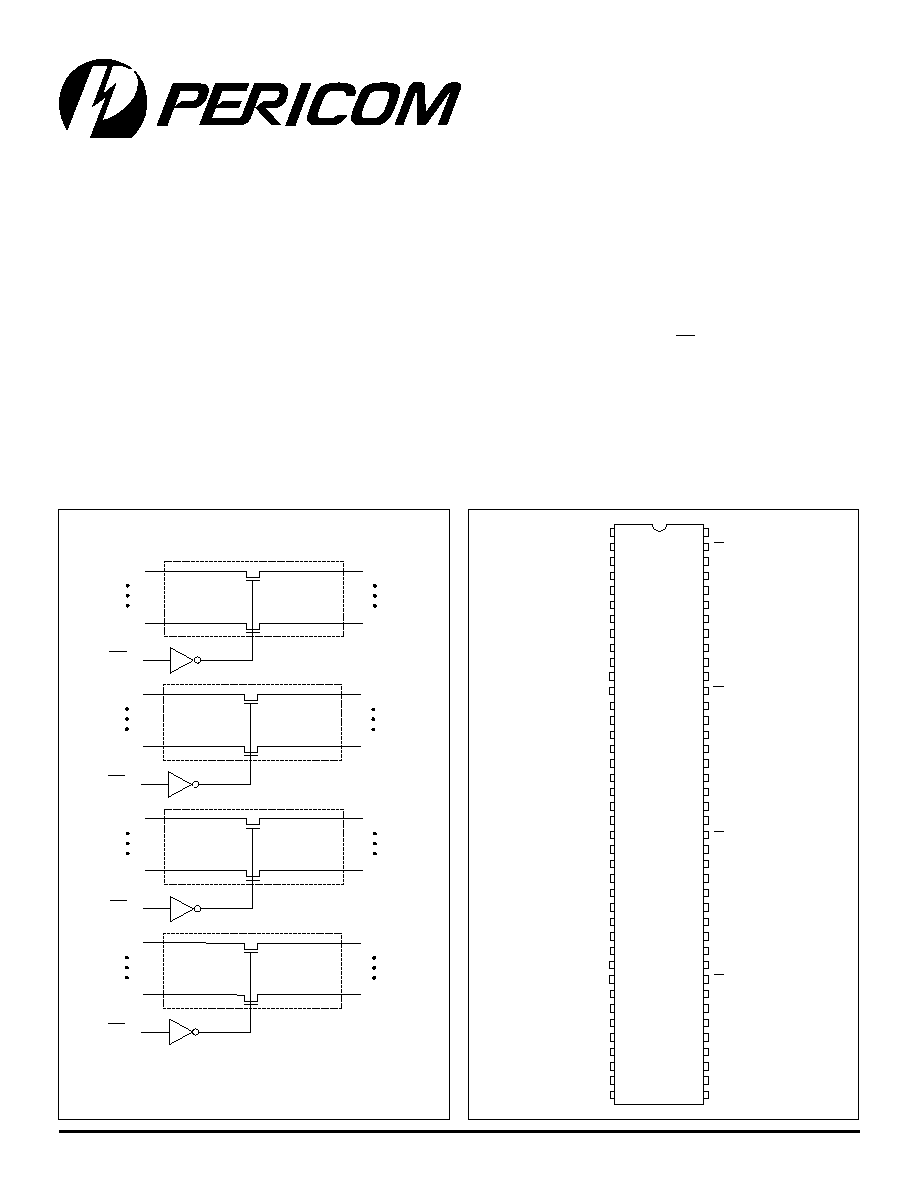
Product Description
Pericom Semiconductors PI3VT series of logic circuits are produced
using the Companys advanced submicron CMOS technology,
achieving industry leading performance.
The PI3VT34X245, is a 2.5V or 3.3V 8-bit, 2-port bus switch, is
designed with a low ON resistance (5 ohms). The switches are turned
ON or enabled by the Bus Enable (BEn) input signal.
Given a 3.3V supply and an input voltage of 3.3V, the switch
translates to an output voltage of 2.5V. Similarly, when operated with
a 2.5V supply and given 2.5V inputs, the device translates the
outputs to 1.8V.
Logic Block Diagram
Product Pin Configuration
Product Features
Near zero propagation delay
Low ON resistance switches connect inputs to outputs
2.5V Supply Voltage Operation
2.5V or 1.8V switching
Packages available:
80-pin, 150 mil wide plastic BQSOP (B)
Applications
3.3V to 2.5V level shifting (voltage translation)
2.5V to 1.8V level shifting (voltage translation)
80-Pin
B
PI3VT34X245
32-Bit, 2-Port, Low Voltage
Translator Bus Switch
12345678901234567890123456789012123456789012345678901234567890121234567890123456789012345678901212345678901234567890123456789012123456789012
12345678901234567890123456789012123456789012345678901234567890121234567890123456789012345678901212345678901234567890123456789012123456789012
BE1
A7
A0
B7
B0
BE2
A15
A8
B15
B8
BE3
A23
A16
B23
B16
BE4
A31
A24
B31
B24
2
PS8531 03/19/01
12345678901234567890123456789012123456789012345678901234567890121234567890123456789012345678901212345678901234567890123456789012123456789012
12345678901234567890123456789012123456789012345678901234567890121234567890123456789012345678901212345678901234567890123456789012123456789012
12345678901234567890123456789012123456789012345678901234567890121234567890123456789012345678901212345678901234567890123456789012123456789012
12345678901234567890123456789012123456789012345678901234567890121234567890123456789012345678901212345678901234567890123456789012123456789012
PI3VT34X245
32-Bit, 2-Port, Low Voltage
Translator Bus Switch
Storage Temperature ........................................................65�C to +150�C
Ambient Temperature with Power Applied ......................... 40�C to +85�C
Supply Voltage to Ground Potential .........................................0.5V to +4.6V
DC Input Voltage .................................................................. 0.5V to +5.5V
DC Output Current ............................................................................120mA
Power Dissipation ................................................................................ 0.5W
Note:
Stresses greater than those listed under MAXIMUM
RATINGS may cause permanent damage to the device.
This is a stress rating only and functional operation of
the device at these or any other conditions above those
indicated in the operational sections of this specifica-
tion is not implied. Exposure to absolute maximum
rating conditions for extended periods may affect reli-
ability.
Maximum Ratings
(Above which the useful life may be impaired. For user guidelines, not tested.)
s
r
e
t
e
m
a
r
a
P
n
o
it
p
i
r
c
s
e
D
s
n
o
it
i
d
n
o
C
t
s
e
T
)
1
(
.
n
i
M
.
p
y
T
)
2
(
.
x
a
M
s
ti
n
U
V
H
I
e
g
a
tl
o
V
H
G
I
H
t
u
p
n
I
l
e
v
e
L
H
G
I
H
ci
g
o
L
d
e
e
t
n
a
r
a
u
G
8
.
1
V
C
C
V
3
.
0
+
V
V
L
I
e
g
a
tl
o
V
W
O
L
t
u
p
n
I
l
e
v
e
L
W
O
L
ci
g
o
L
d
e
e
t
n
a
r
a
u
G
5
.
0
8
.
0
I
H
I
t
n
e
rr
u
C
H
G
I
H
t
u
p
n
I
V
C
C
V
,.
x
a
M
=
N
I
V
=
C
C
1
�
A
�
I
L
I
t
n
e
rr
u
C
W
O
L
t
u
p
n
I
V
C
C
V
,.
x
a
M
=
N
I
D
N
G
=
1
�
I
H
Z
O
t
n
e
rr
u
C
t
u
p
t
u
O
e
c
n
a
d
e
p
m
I
h
g
i
H
0
B
,
A
V
C
C
1
�
R
N
O
e
c
n
a
t
si
s
e
R
N
O
h
c
ti
w
S
V
C
C
V
,.
n
i
M
=
N
I
I
,
V
0
.
0
=
N
O
A
m
8
=
5
8
V
C
C
V
,.
n
i
M
=
N
I
I
,
V
7
.
1
=
N
O
A
m
8
=
0
1
2
2
V
C
C
V
,
V
3
.
2
=
N
I
I
,
V
0
.
0
=
N
O
A
m
8
=
6
9
V
C
C
V
,
V
3
.
2
=
N
I
I
,
V
3
.
1
=
N
O
A
m
8
=
5
2
0
3
V
P
e
g
a
tl
o
V
s
s
a
P
V
N
I
V
=
C
C
I
,
V
3
.
3
=
T
U
O
A
�
5
=
3
.
2
5
.
2
9
.
2
V
V
N
I
V
=
C
C
I
,
V
5
.
2
=
T
U
O
A
�
5
=
8
.
1
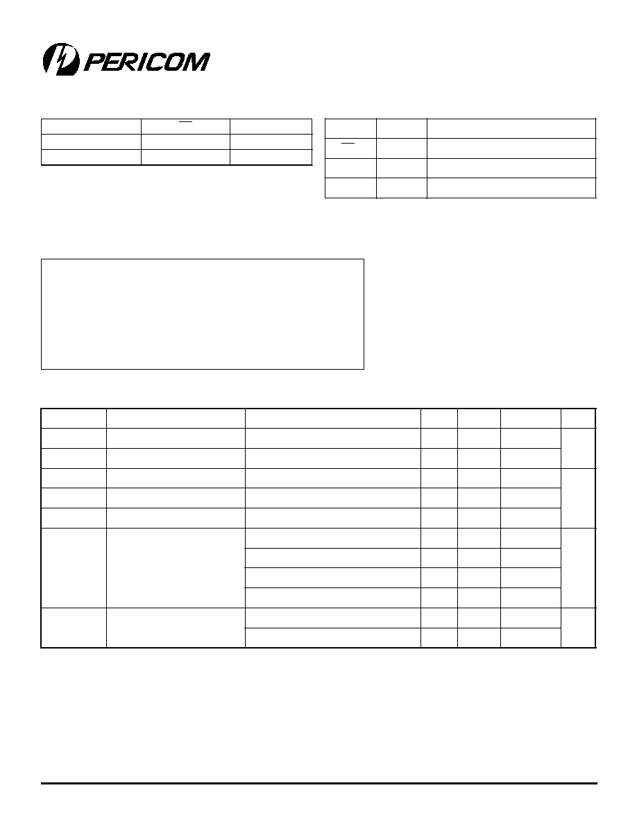
DC Electrical Characteristics
(Over Operating Range, T
A
= 40�C to +85�C, V
CC
= 3.3V �10%)
Function
BE
N
A031
Disconnect
H
Hi-Z
Connect
L
B031
Truth Table
(1)
Notes:
1. H = High Voltage Level
L = Low Voltage Level
Hi-Z = High Impedance
e
m
a
N
n
i
P
O
/
I
n
o
it
p
i
r
c
s
e
D
E
B
N
I
)
W
O
L
e
v
it
c
A
(
t
u
p
n
I
el
b
a
n
E
s
u
B
1
3
A
-
0
A
O
/I
A
s
u
B
1
3
B
-
0
B
O
/I
B
s
u
B
Product Pin Description

PI3VT34X245
32-Bit, 2-Port, Low Voltage
Translator Bus Switch
3
PS8531 03/19/01
12345678901234567890123456789012123456789012345678901234567890121234567890123456789012345678901212345678901234567890123456789012123456789012
12345678901234567890123456789012123456789012345678901234567890121234567890123456789012345678901212345678901234567890123456789012123456789012
12345678901234567890123456789012123456789012345678901234567890121234567890123456789012345678901212345678901234567890123456789012123456789012
12345678901234567890123456789012123456789012345678901234567890121234567890123456789012345678901212345678901234567890123456789012123456789012
Power Supply Characteristics
Notes:
1. For Max. or Min. conditions, use appropriate value specified under Electrical Characteristics for the applicable device.
2. Typical values are at V
CC
= 3.3V, +25�C ambient.
3. Per driven input (control input only); A and B pins do not contribute to
I
CC
.
Switching Characteristics over 3.3V �0.3V Operating Range
Capacitance
(T
A
= 25�C, f = 1 MHz)
Notes:
1. For Max. or Min. conditions, use appropriate value specified under Electrical Characteristics for the applicable device type.
2. Typical values are at V
CC
= 3.3V, T
A
= 25�C ambient and maximum loading.
3. Not more than one output should be shorted at one time. Duration of the test should not exceed one second.
4. Measured by the voltage drop between A and B pin at indicated current through the switch. ON resistance is determined
by the lower of the voltages on the two (A,B) pins.
5. This parameter is determined by device characterization but is not production tested.
s
r
e
t
e
m
a
r
a
P
)
5
(
n
o
it
p
i
r
c
s
e
D
s
n
o
it
i
d
n
o
C
t
s
e
T
.
p
y
T
s
ti
n
U
C
N
I
e
c
n
a
ti
c
a
p
a
C
t
u
p
n
I
V
N
I
V
0
=
5
.
3
F
p
C
F
F
O
ff
O
h
c
ti
w
S
,
e
c
n
a
ti
c
a
p
a
C
B
/
A
0
.
5
C
N
O
n
O
h
c
ti
w
S
,
e
c
n
a
ti
c
a
p
a
C
B
/
A
0
.
0
1
s
r
e
t
e
m
a
r
a
P
n
o
it
p
i
r
c
s
e
D
s
n
o
it
i
d
n
o
C
t
s
e
T
)
1
(
.
n
i
M
.
p
y
T
)
2
(
.
x
a
M
s
ti
n
U
I
C
C
r
e
w
o
P
t
n
e
c
s
ei
u
Q
t
n
e
rr
u
C
y
l
p
p
u
S
V
C
C
.
x
a
M
=
V
N
I
V
r
o
D
N
G
=
C
C
2
1
A
�
I
C
C
r
e
p
t
n
e
rr
u
C
y
l
p
p
u
S
H
G
I
H
t
u
p
n
I
V
N
I =
V
3
)
3
(
0
5
r
e
t
e
m
a
r
a
P
s
n
o
it
i
d
n
o
C
t
s
e
T
s
n
o
it
i
d
n
o
C
)
1
(
.
m
o
C
s
ti
n
U
.
n
i
M
.
x
a
M
t
H
L
P
t
L
H
P
y
al
e
D
n
o
it
a
g
a
p
o
r
P
)
3
,
2
(
x
B
o
t
x
A
,
C
L
F
p
0
5
=
R
L
s
m
h
o
0
0
5
=
5
2
.
0
s
n
t
H
Z
P
t
L
Z
P
x
B
r
o
x
A
o
t
E
B
;
e
m
i
T
el
b
a
n
E
s
u
B
C
L
F
p
0
5
=
R
L
s
m
h
o
0
0
5
=
s
m
h
o
0
0
5
=
R
5
.
1
5
.
6
t
Z
H
P
t
Z
L
P
x
B
r
o
x
A
o
t
E
B
;
e
m
i
T
el
b
a
si
D
s
u
B
5
.
1
5
.
5
4
PS8531 03/19/01
12345678901234567890123456789012123456789012345678901234567890121234567890123456789012345678901212345678901234567890123456789012123456789012
12345678901234567890123456789012123456789012345678901234567890121234567890123456789012345678901212345678901234567890123456789012123456789012
12345678901234567890123456789012123456789012345678901234567890121234567890123456789012345678901212345678901234567890123456789012123456789012
12345678901234567890123456789012123456789012345678901234567890121234567890123456789012345678901212345678901234567890123456789012123456789012
PI3VT34X245
32-Bit, 2-Port, Low Voltage
Translator Bus Switch
Pericom Semiconductor Corporation
2380 Bering Drive � San Jose, CA 95131 � 1-800-435-2336 � Fax (408) 435-1100 � http://www.pericom.com
t
r
a
P
e
g
a
k
c
a
P
-
n
i
P
e
r
u
t
a
r
e
p
m
e
T
B
5
4
2
X
4
3
T
V
3
I
P
)
B
(
P
O
S
Q
B
-
0
8
C
�
5
8
+
o
t
C
�
0
4
Ordering Information
80-pin BQSOP package (Q)
3.80
4.00
0.254
.0197
0.50
5�
Gauge Plane
.150
.157
X.XX
X.XX
DENOTES DIMENSIONS
IN MILLIMETERS
.228
.244
5.80
6.20
.010
.063
.010
.016
0.254
0.406
0.803
0.811
20.40
20.60
.007
.010
0.17
0.27
40
80
x 45�
41
1
.019
1.60
.002
.009
0.05
0.25
.078
2.0
5�
.019
.029
0.50
0.75
.008 NOM
0.203
0.50
REF
BSC
Max
Nom
BSC
Notes:
1. See test circuit and waveforms.
2. This parameter is guaranteed but not tested on Propagation Delays.
3. The bus switch contributes no propagational delay other than the RC delay of the ON resistance of the switch and the load capacitance.
The time constant for the switch alone is of the order of 0.25ns for 50pF load. Since this time constant is much smaller than the rise/fall
times of typical driving signals, it adds very little propagational delay to the system. Propagational delay of the bus switch when used
in a system is determined by the driving circuit on the driving side of the switch and its interaction with the load on the driven side.
Switching Characteristics over 2.5V �0.2V Operating Range
r
e
t
e
m
a
r
a
P
s
n
o
it
i
d
n
o
C
t
s
e
T
s
n
o
it
i
d
n
o
C
)
1
(
.
m
o
C
s
ti
n
U
.
n
i
M
.
x
a
M
t
H
L
P
t
L
H
P
y
al
e
D
n
o
it
a
g
a
p
o
r
P
)
3
,
2
(
x
B
o
t
x
A
,
C
L
F
p
0
5
=
R
L
s
m
h
o
0
0
5
=
5
2
.
0
s
n
t
H
Z
P
t
L
Z
P
x
B
r
o
x
A
o
t
E
B
;
e
m
i
T
el
b
a
n
E
s
u
B
C
L
F
p
0
5
=
R
L
s
m
h
o
0
0
5
=
s
m
h
o
0
0
5
=
R
5
.
1
8
.
9
t
Z
H
P
t
Z
L
P
x
B
r
o
x
A
o
t
E
B
;
e
m
i
T
el
b
a
si
D
s
u
B
5
.
1
8
.
9