1
PS8369B 12/15/01
1
1
2
3
4
5
6
7
GND
8
9
10
11
12
13
14
15
16
17
18
19
20
21
22
23
24
48
47
46
45
44
43
42
41
40
39
38
37
36
35
34
33
32
31
30
29
28
27
26
25
1
A
1 2
A
BIASV
1
A
1
5
A
1
A
1
7
A
1
A
8
1 9
A
1 10
A
2 1
A
2
2
A
V
CC
2
3
A
2
4
A
2
5
A
2
6
A
2
7
A
2
8
A
2
9
A
2
10
A
1
B
5
1
B
1
1
O
E
1 2
B
1 3
B
1
B
4
GND
1
B
6
1 7
B
1
8
B
1
B
9
1
B
10
GND
2 2
B
2 1
B
2
3
B
GND
2 4
B
2
B
5
2 6
B
2
B
7
2
B
8
2 9
B
2
B
10
2
O
E
1
A
3
4
6
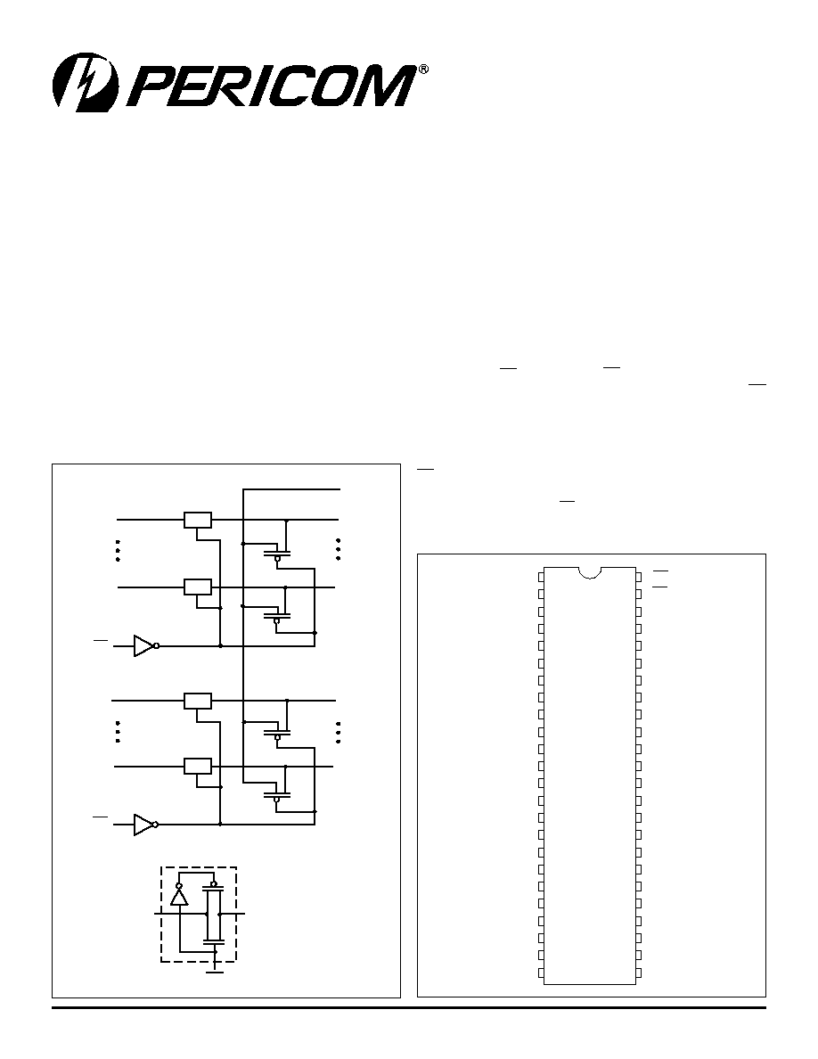
Product Description
Pericom Semiconductors PI5C series of logic circuits are produced
using the companys advanced submicron CMOS technology.
The PI5C16215C provides 20-bits of high-speed bus switching. The
low on-state resistance of the switch allows connections to be made
with minimal propagation delay. The device also precharges the
B-port to a user-selectable bias voltage (BIASV) to minimize live-
insertion noise. The device incorporates an internal charge pump
to handle input undershoot of up to 1.5V and 25ns width.
The device is organized as dual 10-bit bus switches with individual
output-enable (OE) inputs. When OE is low, the corresponding
10-bit bus switch is on and port A is connected to port B. When OE
is high, the switch is open, a high-impedance state exists between
the two ports, and port B is precharged to BIASV through the
equivalent of a 10-k ohm resistor.
To ensure the high-impedance state on power up or power down,
OE should be tied to V
CC
through a pullup resistor; the minimum
value of the resistor is determined by the current-sinking capability
of the driver connected to OE.
Product Features
Undershoot protection up to 1.5V, 25ns width
Near zero propagation delay
5 Ohm switches connect between two ports
Fast switching speed: 4.5ns max.
Permits hot insertion
Isolation during power-off conditions
B-Port outputs are precharged by bias voltage
to minimize signal distortion during live insertion.
Package options include:
- 48-pin 150-mil wide plastic BQSOP (B)
- 48-pin 240-mil wide plastic TSSOP (A)
Product Pin Configuration
Logic Block Diagram
PI5C16215C
20-Bit, Hot Insertion, BusSwitch with
Precharged Outputs & Undershoot Protection
1A10
1A1
1OE
2A1
2OE
2A10
24
13
47
48
12
2
46
36
35
25
1
BIASV
1B1
1B10
2B1
2B10
SW
SW
SW
SW
B
A
OE
48-Pin
A,B
12345678901234567890123456789012123456789012345678901234567890121234567890123456789012345678901212345678901234567890123456789012123456789012
12345678901234567890123456789012123456789012345678901234567890121234567890123456789012345678901212345678901234567890123456789012123456789012
2
PS8369B 12/15/01
12345678901234567890123456789012123456789012345678901234567890121234567890123456789012345678901212345678901234567890123456789012123456789012
12345678901234567890123456789012123456789012345678901234567890121234567890123456789012345678901212345678901234567890123456789012123456789012
PI5C16215C
20-Bit, Hot Insertion, BusSwitch with
Precharged Outputs & Undershoot Protection
Recommended Operating Conditions
(Over Recommended Operating Free-air Temperature Range)
Storage Temperature ..................................... 65∞C to +150∞C
Supply Voltage Range ........................................ 0.5V to +7V
DC Input Voltage
(1) ......................................................
0.5V to +7V
Input Clamp Current, I
IK
(V
I
<0) ................................. 50mA
DC Output Current ....................................................... 120mA
Power Dissipation
(2) ....................................................................
0.5W
Notes:
1. The input and output negative-voltage ratings may be exceeded
if the input and output clamp-current ratings are observed.
2. The maximum package power dissipation is calculated using a
junction temperatue of 150∞C and a board trace length of 750
mils.
Absolute Maximum Ratings Over Free-Air Temperature Range
(Above which the useful life may be impaired. For user guidelines, not tested.)
Notes:
*
Measured by the voltage drop between the A and B terminals at the indicated current through the switch.
On-state resistance is determined by the lower of the voltages of the two (A or B) terminals.
E This is the increase in supply current for each input that is at the specified TTL voltage level rather the V
CC
or GND.
= All typical values are at V
CC
= 5V, T
A
= 25∞C.
r
e
t
e
m
a
r
a
P
s
n
o
it
i
d
n
o
C
t
s
e
T
.
n
i
M
p
y
T
=
.
x
a
M
s
ti
n
U
V
K
I
V
C
C
V
5
.
4
=
I
I
A
m
8
1
=
8
.
1
V
I
I
V
C
C
V
5
.
5
=
V
I
D
N
G
r
o
V
5
.
5
=
5
±
µ
A
I
O
V
C
C
V
V
4
.
2
=
V
S
A
I
B
V
5
.
4
=
O
0
=
5
2
.
0
A
m
I
C
C
V
C
C
V
5
.
5
=
I
O
0
=
V
I
V
=
C
C
D
N
G
r
o
0
0
1
µ
A
I
C
C
E
s
n
i
p
l
o
rt
n
o
C
V
C
C
V
5
.
5
=
V
t
a
r
e
h
t
O
,
V
4
.
3
t
a
t
u
p
n
i
e
n
O
C
C
D
N
G
r
o
5
.
2
A
m
C
I
s
n
i
p
l
o
rt
n
o
C
V
I
0
r
o
V
3
=
5
.
3
F
p
C
O
)
F
F
O
(
V
O
0
r
o
V
3
=
ff
O
h
c
ti
w
S
5
.
4
r
N
O
*
V
C
C
V
4
=
V
I
=
V
4
.
2
I
I
= 5
1 A
m
9
0
2
m
h
o
V
C
C
V
5
.
4
=
V
I
= ,
0
I
I
= 4
6 A
m
5
.
5
8
V
I
= ,
0
I
I
= 0
3 A
m
5
8
V
I
=
V
4
.
2
I
I
= 5
1 A
m
9
5
1
Note:
Stresses greater than those listed under MAXIMUM RATINGS
may cause permanent damage to the device. This is a stress rating
only and functional operation of the device at these or any other
conditions above those indicated in the operational sections of this
specification is not implied. Exposure to absolute maximum rating
conditions for extended periods may affect reliability.
r
e
t
e
m
a
r
a
P
n
o
it
p
i
r
c
s
e
D
.
n
i
M
.
x
a
M
s
ti
n
U
V
C
C
e
g
a
tl
o
v
y
l
p
p
u
S
4
5
.
5
V
V
S
A
I
B
e
g
a
tl
o
v
y
l
p
p
u
S
3
.
1
V
C
C
V
H
I
e
g
a
tl
o
v
t
u
p
n
i
l
e
v
e
L
-
h
g
i
H
2
V
L
I
e
g
a
tl
o
v
t
u
p
n
i
l
e
v
el
-
w
o
L
8
.
0
T
A
e
r
u
t
a
r
e
p
m
e
t
ri
a
-
e
e
rf
g
n
it
a
r
e
p
O
0
4
5
8
C
∞
Electrical Characteristics
(Over Recommended Operating Free-air Temperature Range)
3
PS8369B 12/15/01
12345678901234567890123456789012123456789012345678901234567890121234567890123456789012345678901212345678901234567890123456789012123456789012
12345678901234567890123456789012123456789012345678901234567890121234567890123456789012345678901212345678901234567890123456789012123456789012
PI5C16215C
20-Bit, Hot Insertion, BusSwitch with
Precharged Outputs & Undershoot Protection
Switching Characteristics
(Over Recommended Operating Free-air Temperature Range, C
L
= 50pF)
Notes:
1. This parameter is warranted but not production tested. The propagation delay is based on the RC time constant of the typical on-state
resistance of the switch and a load capacitance of 50pF, when driven by an ideal voltage source (zero output impedance).
Parameter Measurements
VOLTAGE WAVEFORMS
PROPAGATION DELAY TIMES
VOLTAGE WAVEFORMS
ENABLE AND DISABLE TIMES
Notes:
1. C
L
includes probe and jig capacitance.
2. Waveform 1 is for an output with internal conditions such that the output is LOW except when disabled by the output control.
Waveform 2 is for an output with internal conditions such that the output is HIGH except when disabled by the output control.
3. All input pulses are supplied by generators having the following characteristics: PRR<10MHz, Z
O
= 50
, t
r
2.5ns, t
f
2.5ns.
4. The outputs are measured one at a time with one transition per measurement.
5. t
PLZ
and t
PHZ
are the same as t
dis
.
6. t
PZL
and t
PZH
are the same as t
en
.
7. t
PLH
and t
PHL
are the same as t
pd
.
t
PZL
Output
Control
(Low Level
Enabling)
0V
1.5V
1.5V
1.5V
1.5V
t
PLZ
t
PHZ
V
OL
3.5V
0V
t
PZH
+0.3V
-0.3V
Output
Waveform 1
S1 at 6V
(see Note 2)
Output
Waveform 2
S1 at Open
(see Note 2)
V
OH
V
OH
V
OL
3V
t
s
e
T
1
S
d
p
t
n
e
p
O
t
Z
L
P
t/
L
Z
P
V
7
t
Z
H
P
t/
H
Z
P
n
e
p
O
r
e
t
e
m
a
r
a
P
s
n
o
it
i
d
n
o
C
t
s
e
T
m
o
r
F
)t
u
p
n
I
(
o
T
)t
u
p
t
u
O
(
V
C
C
V
5
.
0
±
V
5
=
V
C
C
V
4
=
s
ti
n
U
.
n
i
M
.
x
a
M
.
n
i
M
.
x
a
M
t
D
P
B
r
o
A
A
r
o
B
5
2
.
0
5
2
.
0
s
n
t
H
Z
P
D
N
G
=
V
S
A
I
B
N
O
B
r
o
A
1
.
3
5
6
t
L
Z
P
V
3
=
V
S
A
I
B
0
.
3
5
6
t
Z
H
P
D
N
G
=
V
S
A
I
B
N
O
B
r
o
A
0
.
2
5
5
.
5
t
Z
L
P
V
3
=
V
S
A
I
B
3
5
5
.
5
Input
t
PLH
t
PHL
3V
1.5V
1.5V
1.5V
1.5V
0V
Output
V
OH
V
OL
Truth Table
E
O
n
o
it
c
n
u
F
L
tr
o
p
B
=
tr
o
p
A
H
V
S
A
I
B
=
tr
o
P
B
,
Z
=
tr
o
p
A
500
ohm
500
ohm
7V
Open
GND
S1
LOAD CIRCUIT
From Output
Under Test
C
L
= 50pF
(See note 1)
4
PS8369B 12/15/01
12345678901234567890123456789012123456789012345678901234567890121234567890123456789012345678901212345678901234567890123456789012123456789012
12345678901234567890123456789012123456789012345678901234567890121234567890123456789012345678901212345678901234567890123456789012123456789012
PI5C16215C
20-Bit, Hot Insertion, BusSwitch with
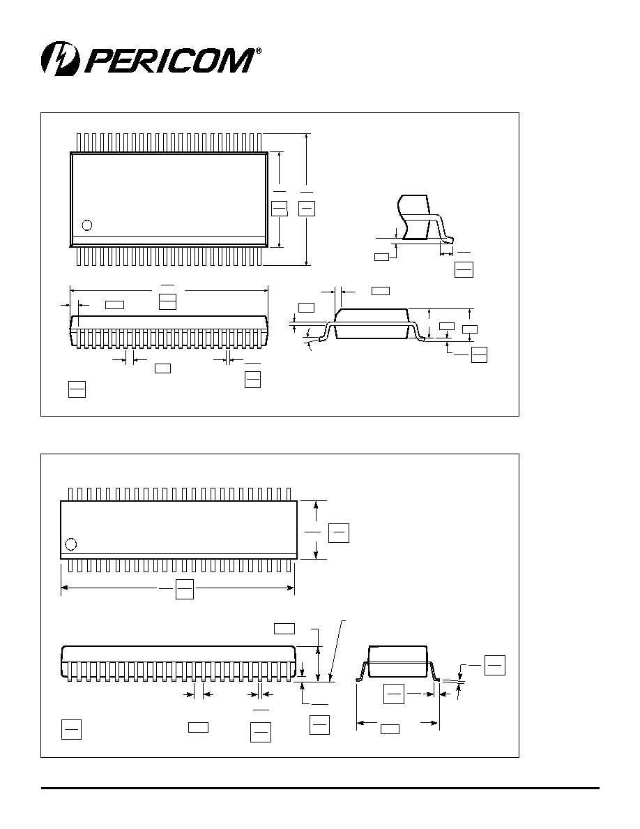
Precharged Outputs & Undershoot Protection
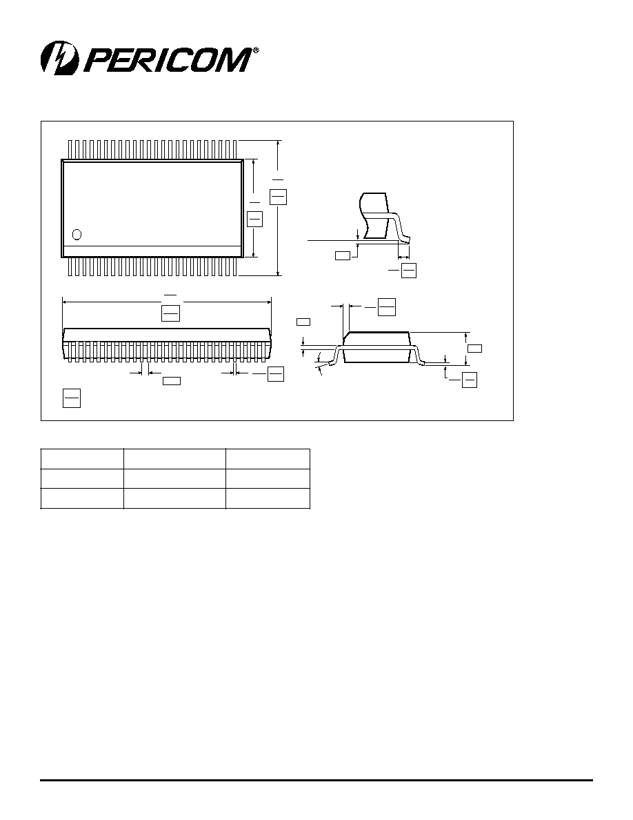
.014
.0157 BSC
0.40
0.356
.008 0.20
.002
.009
5
∞
0.05
0.25
.079
2.0
.010 0.25
Gauge Plane
.150
.157
X.XX
X.XX
DENOTES DIMENSIONS
IN MILLIMETERS
3.80
4.00
.228
.244
5.80
6.20
.020
.029
0.50
0.75
.063
1.60
.015 0.381
.386
.394
9.80
10.00
.0051
.009
0.13
0.23
1
48
x 45
∞
BSC
Nom
Max
Nom
REF
.236
.244
.488
.496
.002
.006
SEATING PLANE
.007
.010
.0197
BSC
.004
.008
.319
1
48
12.4
12.6
6.0
6.2
0.50
0.17
0.27
8.1
0.05
0.15
0.09
0.20
X.XX
X.XX
DENOTES DIMENSIONS
IN MILLIMETERS
.018
.030
0.45
0.75
.047
1.20 Max
BSC
48-pin BQSOP (B)
48-pin TSSOP (A)
5
PS8369B 12/15/01
12345678901234567890123456789012123456789012345678901234567890121234567890123456789012345678901212345678901234567890123456789012123456789012
12345678901234567890123456789012123456789012345678901234567890121234567890123456789012345678901212345678901234567890123456789012123456789012
PI5C16215C
20-Bit, Hot Insertion, BusSwitch with
Precharged Outputs & Undershoot Protection
t
r
a
P
e
g
a
k
c
a
P
-
n
i
P
h
t
d
i
W
B
C
5
1
2
6
1
C
5
I
P
)
8
4
B
(
P
O
S
Q
B
-
8
4
li
m
-
0
5
1
A
C
5
1
2
6
1
C
5
I
P
)
8
4
A
(
P
O
S
S
T
-
8
4
li
m
-
0
4
2
Ordering Information
Pericom Semiconductor Corporation
2380 Bering Drive ∑ San Jose, CA 95131 ∑ 1-800-435-2336 ∑ Fax (408) 435-1100 ∑ http://www.pericom.com
0.20
0.51
1.01
0.25
0.381
0.635
.008
.008
.016
0-8∞
0.20
0.40
.110 2.79
.010
Gauge Plane
.02
.04
.015
.025
x 45∞
.025 BSC
0.635
.291
.299
X.XX
X.XX
DENOTES DIMENSIONS
IN MILLIMETERS
7.39
7.59
.395
.420
10.03
10.67
.620
.630
15.75
16.00
.008
.0135
0.20
0.34
1
48
Nom.
Max
48-pin SSOP (V)
Applications Information
Logic Inputs
The logic control inputs can be driven up to +5.5V regardless of the
supply voltage. For example, given a +5.0V supply, IN may be driven
low to 0V and high to 5.5V. Driving IN Rail-to-RailÆ minimizes power
consumption.
Power-Supply Sequencing
Proper power-supply sequencing is recommended for all CMOS
devices. Always apply V
CC
before applying signals to the bias
voltage pin and the input/output or control pins.
Rail-to-Rail is a registered trademark of Nippon Motorola, Ltd