 | –≠–ª–µ–∫—Ç—Ä–æ–Ω–Ω—ã–π –∫–æ–º–ø–æ–Ω–µ–Ω—Ç: PI5C6800 | –°–∫–∞—á–∞—Ç—å:  PDF PDF  ZIP ZIP |

1
PS8194E 09/13/04
V
CC
B
1
B
2
B
3
B
4
B
5
B
6
B
7
B
8
B
9
B
10
BIASV
1
2
3
4
5
6
7
8
9
10
11
12
24
23
22
21
20
19
18
17
16
15
14
13
ON
A
1
A
2
A
3
A
4
A
5
A
6
A
7
A
8
A
9
A
10
GND
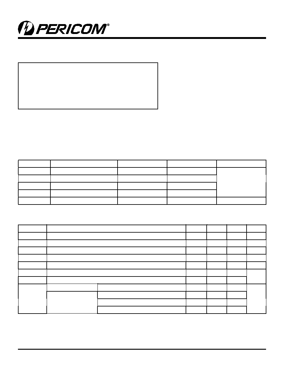
Pin Configuration
Notes:
1. H = High Voltage Level, L = Low Voltage Level
Block Diagram
PI5C6800
10-Bit Bus Switch with
Precharged Outputs
Description
Pericom's Semiconductor's PI5C6800 is a 10-bit bus switch with
low On-State resistance. The bus switch creates no additional
propagation delay.
The switch is turned on by a single enable (ON) input. When ON
is LOW, the switch is on and port A is connnected to port B. When
ON is HIGH, the switch between port A and port B is open and
the B port is precharged to BIASV through the equivalent of a
10-k resistor.
Features
∑ Near-Zero propagation delay
∑ 5 switch connection between two ports
∑ Ultra-low quiescent power (0.2µA typ.)
∑ Ideally suited for notebook applications
∑ A port is hot swapable
∑ Packaging (Pb-free & Green available):
≠ 24-pin 150-mil wide QSOP (Q)
≠ 24-pin 173-mil wide TSSOP (L)
ON
A
10
A
1
13
23
14
B
1
B
10
Truth Table
(1)
Function
ON
B1 - B1
Connect
L
A1- A1
Precharge
H
B
IASV
2
PS8194E 09/13/04
PI5C6800
10-Bit Bus Switch with
Precharged Outputs
Storage Temperature .....................................................≠65∞C to +150∞C
Supply Voltage Range.........................................................≠0.5V to +7V
DC Input Voltage
(2)
.............................................................≠0.5V to +7V
Input Clamp Current, I
IK
(V
1
<0) ..................................................≠50mA
DC Output Current........................................................................120mA
Power Dissipation
(3)
........................................................................0.5W
Notes:
1. Stresses greater than those listed under MAXIMUM RATINGS may cause permanent damage to the device. This is a stress rating only and
functional operation of the device at these or any other conditions above those indicated in the operational sections of this specification is not
implied. Exposure to absolute maximum rating conditions for extended periods may affect reliability.
2. The input and output negative-voltage ratings may be exceeded if the input and output clamp-current ratings are observed.
3. The maximum package power dissipation is calculated using a junction temperatue of 150∞C and a board trace length of 750 mils.
Absolute Maximum Ratings Over Free-Air Temperature Range
(1)
(Above which the useful life may be impaired. For user guidelines, not tested.)
Recommended Operating Conditions
Parameters
Description
Min.
Typ.
Units
V
CC
Supply Voltage
4
5.5
V
BIASV
Supply Voltage
1.3
V
CC
V
IH
High-level input voltage
2
V
IL
Low-level input voltage
0.8
T
A
Operating free-air voltage
-40
85
∞C
Electrical Characteristics
(Over Recommended Operating Free-air Temperature Range)
Parameters
Test Condidtion
Min.
Typ.
(3)
Max.
Units
V
IK
V
CC
= 4.5V, I
I
= -18mA
-1.2
V
I
I
V
CC
= 5.5V, V
I
= 5.5V or GND
±5
µA
I
O
V
CC
= 4.5V, BIASV = 2.4V, V
O
= 0
-0.20
mA
I
CC
V
CC
= 5.5V, I
O
= 0, V
I
= V
CC
or GND
3
µA
I
CC
(2)
V
CC
= 3.6V, One input at 2.7V Other at V
CC
or GND
2.5
mA
C
IN
V
I
= 3V or 0
3.5
pF
C
OFF
V
O
= 3V or 0, Switch Off
4.5
R
ON
(1)
V
CC
= 4V
V
I
= 2.4V, I
I
= 15mA
14
22
V
CC
= 4.5V
V
I
= 0V, I
I
= 64mA
5
7
V
I
= 0V, I
I
= 30mA
5
7
V
I
= 2.4V, I
I
= 15mA
10
15
Notes:
1. Measured by the voltage drop between the A and B terminals at the indicated current through the switch. On-State resistance is determined by
the lower of the voltages of the two (A or B) terminals.
2. This is the increase in supply current for control input.
3. All typical values are at V
CC
= 5V, T
A
= 25∞C.

3
PS8194E 09/13/04
PI5C6800
10-Bit Bus Switch with
Precharged Outputs
Notes:
1. This parameter is warranted but not production tested. The propagation delay is based on the RC time constant of the typical On-State resis-
tance of the switch and a load capacitance of 50pF, when driven by an ideal voltage source (zero output impedance).
Parameter Measurements
VOLTAGE WAVEFORMS
PROPAGATION DELAY TIMES
VOLTAGE WAVEFORMS
ENABLE AND DISABLE TIMES
Notes:
1. C
L
includes probe and jig capacitance.
2. Waveform 1 is for an output with internal conditions such that the output is LOW except when disabled by the output control.
Waveform 2 is for an output with internal conditions such that the output is HIGH except when disabled by the output control.
3. All input pulses are supplied by generators having the following characteristics: PRR<10MHz, Z
O
= 50, t
r
2.5ns, t
f
2.5ns.
4. The outputs are measured one at a time with one transition per measurement.
5. t
PLZ
and t
PHZ
are the same as t
dis
.
6. t
PZL
and t
PZH
are the same as t
en
.
7. t
PLH
and t
PHL
are the same as t
pd
.
t
PZL
Output
Control
(Low Level
Enabling)
0V
1.5V
1.5V
1.5V
1.5V
t
PLZ
t
PHZ
V
OL
3.5V
0V
t
PZH
+0.3V
-0.3V
Output
Waveform 1
S1 at 6V
(see Note 2)
Output
Waveform 2
S1 at Open
(see Note 2)
V
OH
V
OH
V
OL
3V
500
500
7V
Open
GND
S1
LOAD CIRCUIT
From Output
Under Test
CL = 50pF
(See note 1)
Input
t
PLH
t
PHL
3V
1.5V
1.5V
1.5V
1.5V
0V
Output
V
OH
V
OL
Switching Characteristics
Over Recommended Operating Free-air Temperature Range, C
L
= 50pF.
Parameter
Test Conditions
From (Input)
To (Input)
V
CC
= 5V ±0.5V
V
CC
= 4V
Units
Min.
Max.
Min.
Max.
t
PD
(1)
A or B
B or A
0.25
0.25
ns
t
PZH
BIASV = GND
ON
A or B
3.1
5
6
t
PZL
BIASV = 3V
3.6
5
6
t
PHZ
BIAS = GND
ON
A or B
2.7
5
5.5
t
PLZ
BIAS = 3V
3
5
5.5
Test
S1
t
PD
Open
t
PLZ
/t
PZL
7V
t
PHZ
/t
PZH
Open
4
PS8194E 09/13/04
PI5C6800
10-Bit Bus Switch with
Precharged Outputs
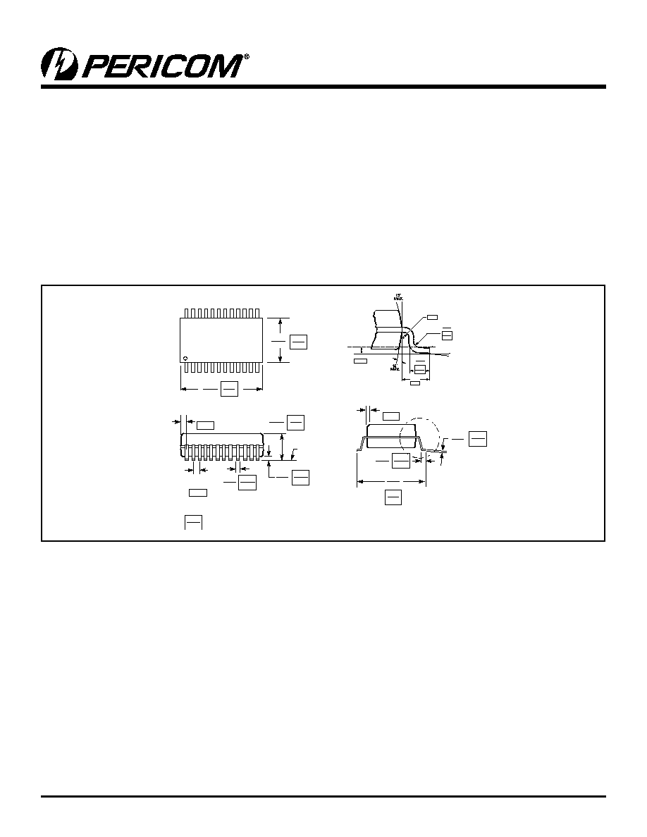
Packaging Mechanical: 24-pin QSOP (Q)
.337
.344
.053
.069
.004
.010
SEATING
PLANE
.025
typical
.007
.010
.228
.244
1
24
.150
.157
.016
.050
X.XX
X.XX
DENOTES DIMENSIONS
IN MILLIMETERS
0.635
8.56
8.74
1.35
1.75
5.79
6.20
0.406
1.27
0.101
0.254
.008
.012
0.203
0.305
3.81
3.99
0.178
0.254
.033
0.84
0.38
.015 x 45∞
Detail A
Detail A
.008
0.20
MIN.
Guage Plane
.010
0.254
.041
1.04
REF
.016
.035
0.41
0.89
0∞-6∞
.008
.013
0.20
0.33
Applications Information
Logic Inputs
The logic control inputs can be driven up to +5.5V regardless of the supply voltage. For example, given a +5.0V supply, IN may be
driven low to 0V and high to 5.5V. Driving IN Rail-to-RailÆ minimizes power consumption.
Power-Supply Sequencing
Proper power-supply sequencing is recommended for all CMOS devices. Always apply V
CC
before applying signals to the input/
output or control pins.
Rail-to-Rail is a registered trademark of Nippon Motorola, Ltd

5
PS8194E 09/13/04
PI5C6800
10-Bit Bus Switch with
Precharged Outputs
Pericom Semiconductor Corporation 1-800-435-2336 ∑ www.pericom.com
Ordering Information
Ordering Code
Package Code
Package Description
PI5C6800L
L
24-Pin 173-mil TSSOP
PI5C6800LE
L
Pb-free & Green, 24-Pin 173-mil TSSOP
PI5C6800Q
Q
24-Pin 150-mil QSOP
PI5C6800QE
Q
Pb-free & Green, 24-Pin 150-mil QSOP
Notes:
1. Thermal characteristics can be found on the web at www.pericom.com/packaging/
2. Number of Transistors = TBD
Packaging Mechanical: 24-pin TSSOP (L)
.303
.311
.047
1.20
.002
.006
SEATING
PLANE
.0256
BSC
.018
.030
.004
.008
.252
BSC
1
24
.169
.177
X.XX
X.XX
DENOTES CONTROLLING
DIMENSIONS IN MILLIMETERS
0.05
0.15
6.4
0.45
0.75
0.09
0.20
4.3
4.5
7.7
7.9
0.65
0.19
0.30
.007
.012
Max