
1
PS8590C 09/22/04
12345678901234567890123456789012123456789012345678901234567890121234567890123456789012345678901212345678901234567890123456789012123456789012
12345678901234567890123456789012123456789012345678901234567890121234567890123456789012345678901212345678901234567890123456789012123456789012
PI6C2972
Description
The PI6C2972 are 3.3V compatible, PLL based clock driver devices
targeted for high-performance CISC or RISC processor based sys-
tems. With output frequencies of up to 125 MHz and skews of 550ps
the PI6C2972 are ideally suited for most synchronous systems. The
devices offer twelve low skew outputs plus a feedback and sync
output for added flexibility and ease of system implementation.
The PI6C2972 features an extensive level of frequency programma-
bility between the 12 outputs as well as the input vs output
relationships. Using the select lines output frequency ratios of 1:1,
2:1, 3:1, 3:2, 4:1, 4:3, 5:1, 5:2, 5:3, 6:1 and 6:5 between outputs can be
realized by pulsing low one clock edge prior to the coincident edges
of the Qa and Qc outputs. The Sync output will indicate when the
coincident rising edges of the above relationships will occur. The
Power≠On Reset ensures proper programming if the frequency
select pins are set at power up. If the fselFB2 pin is held high, it may
be necessary to apply a reset after power≠up to ensure synchroni-
zation between the QFB output and the other outputs. The internal
power≠on reset is designed to provide this function, but with
power≠up conditions being dependent, it is difficult to guarantee.
All other conditions of the fsel pins will automatically synchronize
during PLL lock acquisition.
The PI6C2972 offers a very flexible output enable/disable scheme.
Note that all of the control inputs on the PI6C2972 have internal pull≠
up resistors.
The PI6C2972 is fully 3.3V compatible and requires no external loop
filter components. All inputs accept LVCMOS/LVTTL compatible
levels while the outputs provide LVCMOS levels with the capability
to drive 50-ohm transmission lines. For series terminated lines each
PI6C2972 output can drive two 50-ohm lines in parallel thus effec-
tively doubling the fanout of the device.
Features
∑ Fully Integrated PLL
∑ Output Frequency up to 125 MHz
∑ Compatible with PowerPC and Pentium Microprocessors
∑ 3.3V V
CC
∑ + 100ps Typical Cycle≠to≠Cycle Jitter
∑ Packaging (Pb-free & Green available):
- 52-pin LQFP (FC)
Low Voltage PLL Clock Driver
Pin Configuration
40
41
42
43
44
45
46
47
48
49
50
51
52
26
25
24
23
22
21
20
19
18
17
16
15
14
1 2 3 4 5 6 7 8 9 10 11 12 13
39 38 37 36 35 34 33 32 31 30 29 28 27
fselb1
fselb0
fsela1
fsela0
Qa3
VCCO
Qa2
GNDO
Qa1
VCCO
Qa0
GND0
VCO_Sel
fselFB1
QSync
GNDO
Qc0
VCCO
Qc1
fselc0
fselc1
Qc2
VCCO
Qc3
GND0
Inv_Clk
GNDO
Qb0
VCCO
Qb1
GND0
Qb2
VCCO
Qb3
Ext_FB
GNDO
QFB
VCCI
fselFB0
GND1
MR/OE
Frz_Clk
Frz_Data
fselFB2
PLL_EN
Ref_Sel
TClk_Sel
TClk0
TClk1
xtal1
xtal2
VCCA

2
PS8590C 09/22/04
12345678901234567890123456789012123456789012345678901234567890121234567890123456789012345678901212345678901234567890123456789012123456789012
12345678901234567890123456789012123456789012345678901234567890121234567890123456789012345678901212345678901234567890123456789012123456789012
PI6C2972
Low Voltage PLL Clock Driver
Block Diagram
VCO
PHASE
DETECTOR
V
Qa1
Qa0
Qa3
Qa2
Qb3
Qb2
Qb1
Qb0
Qc3
Qc2
Qc1
Qc0
QSync
QFB
V
V
V
Sync
Frz
˜2
2
2
2
2
˜4, ˜6, ˜8, ˜12
˜4, ˜6, ˜8, ˜10
˜2, ˜4, ˜6, ˜8
˜4, ˜6, ˜8, ˜10
Sync Pulse
Data Generator
0
D
Q
D
Q
1
Sync
Frz
Sync
Frz
LPF
0
1
0
1
TCLK1
TCLK_Sel
Ext_FB
TCLK0
PLL_En
REF_Sel
VC0_Sel
V
D
Q
fsela0:1
fselb0:1
fselc0:1
fselFBO:1
Frz_Clk
Frz_Data
Inv_Clk
MR/OE
fselFB2
POWER-ON
RESET
Output Disable
Circuitry
V
12
V
D
Q
V
D
Q
D
Q
Sync
Frz
Sync
Frz
xtal_1
xtal_2
V

3
PS8590C 09/22/04
12345678901234567890123456789012123456789012345678901234567890121234567890123456789012345678901212345678901234567890123456789012123456789012
12345678901234567890123456789012123456789012345678901234567890121234567890123456789012345678901212345678901234567890123456789012123456789012
PI6C2972
Low Voltage PLL Clock Driver
Function Table 1
1
a
l
e
s
f
0
a
l
e
s
f
a
Q
1
b
l
e
s
f
0
b
l
e
s
f
b
Q
1
c
l
e
s
f
0
c
l
e
s
f
c
Q
0
0
1
1
0
1
0
1
4
˜
6
˜
8
˜
2
1
˜
0
0
1
1
0
1
0
1
4
˜
6
˜
8
˜
0
1
˜
0
0
1
1
0
1
0
1
2
˜
4
˜
6
˜
8
˜
2
B
F
l
e
s
f
1
B
F
l
e
s
f
0
B
F
l
e
s
f
B
F
Q
0
0
0
0
0
0
1
1
0
1
0
1
4
˜
6
˜
8
˜
0
1
˜
1
1
1
1
0
0
1
1
0
1
0
1
8
˜
2
1
˜
6
1
˜
0
2
˜
n
i
P
l
o
r
t
n
o
C
'
0
'
c
i
g
o
L
'
1
'
c
i
g
o
L
l
e
S
_
O
C
V
l
e
S
_
f
e
R
l
e
S
_
K
L
C
T
n
E
_
L
L
P
E
O
/
R
M
K
L
C
_
v
n
I
2
/
O
C
V
K
L
C
T
0
K
L
C
T
L
L
P
s
s
a
p
y
B
Z
-i
H
t
u
p
t
u
O
/t
e
s
e
R
r
e
t
s
a
M
3
c
Q
,
2
c
Q
d
e
t
r
e
v
n
I
-
n
o
N
O
C
V
l
a
t
X
1
K
L
C
T
L
L
P
e
l
b
a
n
E
s
t
u
p
t
u
O
e
l
b
a
n
E
3
c
Q
,
2
c
Q
d
e
t
r
e
v
n
I
Function Table 2
Function Table 3
s
r
e
t
e
m
a
r
a
P
e
u
l
a
V
t
u
C
l
a
t
s
y
r
C
t
u
C
T
A
l
a
t
n
e
m
a
d
n
u
F
e
c
n
a
n
o
s
e
R
e
c
n
a
n
o
s
e
R
l
e
ll
a
r
a
P
e
c
a
n
r
e
l
o
T
.
q
e
r
F
C
∞
5
2
@
m
p
p
0
0
1
±
y
ti
li
b
a
t
S
.
p
m
e
T
.
q
e
r
F
)
C
∞
0
7
o
t
∞
0
(
m
p
p
5
7
1
±
e
g
n
a
R
g
n
it
a
r
e
p
O
C
∞
0
7
o
t
∞
0
e
c
n
a
ti
c
a
p
a
C
t
n
u
h
S
F
p
7
<
R
S
E
m
h
O
-
0
4
<
l
e
v
e
L
e
v
i
r
D
W
m
5
g
n
i
g
A
)
s
r
a
e
y
3
t
s
ri
F
(
r
a
e
Y
/
m
p
p
5
Crystal Recommendations

4
PS8590C 09/22/04
12345678901234567890123456789012123456789012345678901234567890121234567890123456789012345678901212345678901234567890123456789012123456789012
12345678901234567890123456789012123456789012345678901234567890121234567890123456789012345678901212345678901234567890123456789012123456789012
PI6C2972
Low Voltage PLL Clock Driver
1:1 Mode
2:1 Mode
3:1 Mode
3:2 Mode
4:1 Mode
4:3 Mode
1:6 Mode
fVCO
Qa
Qc
Sync
Qa
Qc
Sync
Qc( 2)
Qa( 6)
Sync
Qa( 4)
Qc( 6)
Sync
Qc( 2)
Qa( 8)
Sync
Qa( 6)
Qc( 8)
Sync
Qa( 12)
Qc( 2)
Sync
Timing Diagrams

5
PS8590C 09/22/04
12345678901234567890123456789012123456789012345678901234567890121234567890123456789012345678901212345678901234567890123456789012123456789012
12345678901234567890123456789012123456789012345678901234567890121234567890123456789012345678901212345678901234567890123456789012123456789012
PI6C2972
Low Voltage PLL Clock Driver
l
o
b
m
y
S
s
n
o
i
t
i
d
n
o
C
c
i
t
s
i
r
e
t
c
a
r
a
h
C
.
n
i
M
.
p
y
T
.
x
a
M
s
t
i
n
U
V
H
I
e
g
a
tl
o
V
H
G
I
H
t
u
p
n
I
0
.
2
6
.
3
V
V
L
I
e
g
a
tl
o
V
W
O
L
t
u
p
n
I
8
.
0
V
H
O
I
H
O
A
m
0
2
=
)
2
(
e
g
a
tl
o
V
H
G
I
H
t
u
p
t
u
O
4
.
2
V
L
O
I
L
O
A
m
0
2
=
)
2
(
e
g
a
tl
o
V
W
O
L
t
u
p
t
u
O
5
.
0
I
N
I
3
e
t
o
N
t
n
e
r
r
u
C
t
u
p
n
I
0
2
1
±
µ
I
C
C
t
n
e
r
r
u
C
y
l
p
p
u
S
t
n
e
c
s
e
i
u
Q
m
u
m
i
x
a
M
0
9
1
5
1
2
A
m
I
A
C
C
V
g
o
l
a
n
A
C
C
t
n
e
r
r
u
C
5
1
0
2
C
N
I
e
c
n
a
ti
c
a
p
a
C
t
u
p
n
I
4
F
p
C
d
p
t
u
p
t
u
O
r
e
P
e
c
n
a
ti
c
a
p
a
C
n
o
it
a
p
i
s
s
i
D
r
e
w
o
P
5
2
Notes:
1. V
CMR
is the difference from the most positive side of the differential input signal. Normal operation is obtained when
the "High" input is within the V
CMR
range and the input lies within the V
PP
specification.
2. The PI6C2972 outputs can drive series or parallel terminated 50 Ohm (or 50 Ohm to V
CC
/2) transmission lines on the
incident edge.
3. Inputs have pull≠up/pull≠down resistors which affect input current.
4. Special thermal handling may be required in some configurations.
l
o
b
m
y
S
r
e
t
e
m
a
r
a
P
.
n
i
M
.
x
a
M
s
t
i
n
U
V
C
C
e
g
a
tl
o
V
y
l
p
p
u
S
3
.
0
≠
6
.
4
V
V
I
e
g
a
tl
o
V
t
u
p
n
I
3
.
0
≠
V
D
D
3
.
0
+
V
I
N
I
t
n
e
r
r
u
C
t
u
p
n
I
0
2
±
A
m
T
R
O
T
S
e
r
u
t
a
r
e
p
m
e
T
e
g
a
r
o
t
S
0
4
≠
5
2
1
C
∞
*Absolute maximum continuous ratings are those values beyond which damage to the device may occur.
Exposure to these conditions or conditions beyond those indicated may adversely affect device reliability.
Functional operation under absolute-maximum-rated conditions is not implied.
DC Characteristics (T
A
= 0∞C to 70∞C, V
CC
= 3.3V ± 5%)
(4)
Absolute Maximum Ratings

6
PS8590C 09/22/04
12345678901234567890123456789012123456789012345678901234567890121234567890123456789012345678901212345678901234567890123456789012123456789012
12345678901234567890123456789012123456789012345678901234567890121234567890123456789012345678901212345678901234567890123456789012123456789012
PI6C2972
Low Voltage PLL Clock Driver
Notes:
7. 50 Ohm transmission line terminated into V
CC
/2
8. tpd is specified for a 50 MHz input reference. The window will shrink/grow proportionally from the minimum limit with shorter/
longer input reference periods. The tpd does not include jitter.
l
o
b
m
y
S
s
n
o
i
t
i
d
n
o
C
s
c
i
t
s
i
r
e
t
c
a
r
a
h
C
.
n
i
M
.
x
a
M
s
t
i
n
U
f
t
,r
t
s
ll
a
F
/
e
s
i
R
t
u
p
n
I
K
L
C
T
0
.
3
s
n
f
e
r
f
5
e
t
o
N
y
c
n
e
u
q
e
r
F
t
u
p
n
I
e
c
n
e
r
e
f
e
R
5
e
t
o
N
5
e
t
o
N
,
0
0
1
z
H
M
C
D
f
e
r
f
e
l
c
y
C
y
t
u
D
t
u
p
n
I
e
c
n
e
r
e
f
e
R
5
2
5
7
%
l
a
t
x
t
y
c
n
e
u
q
e
r
F
r
o
t
a
ll
i
c
s
O
l
a
t
s
y
r
C
0
1
5
2
z
H
M
PLL Input Reference Characteristic (T
A
= 0∞C to 70∞C)
Notes:
5. Maximum input reference frequency is limited by the VCO lock range and the feedback divider or 100 MHz,
minimum input reference frequency is limited by the VCO lock range and the feedback divider.
l
o
b
m
y
S
s
c
i
t
s
i
r
e
t
c
a
r
a
h
C
s
n
o
i
t
i
d
n
o
C
.
n
i
M
.
p
y
T
.
x
a
M
s
t
i
n
U
t
,r
t
f
)
7
e
t
o
N
(
e
m
i
T
ll
a
F
/
e
s
i
R
t
u
p
t
u
O
V
0
.
2
o
t
8
.
0
5
1
.
0
2
.
1
s
n
t
w
p
)
7
e
t
o
N
(
e
l
c
y
C
y
t
u
D
t
u
p
t
u
O
t
E
L
C
Y
C
2
/
0
5
7
≠
t
E
L
C
Y
C
2
/
0
0
5
±
t
E
L
C
Y
C
2
/
0
5
7
+
s
p
t
d
p
y
a
l
e
D
n
o
it
a
g
a
p
o
r
P
=
B
F
Q
,
8
,
7
s
e
t
o
N
˜
8
0
K
L
C
T
1
K
L
C
T
0
7
2
≠
0
3
3
≠
0
3
1
0
7
0
3
5
0
7
4
t
s
o
w
e
k
S
t
u
p
t
u
O
-
o
t
-
t
u
p
t
u
O
7
e
t
o
N
0
5
5
f
O
C
V
e
g
n
a
R
k
c
o
L
O
C
V
7
e
t
o
N
0
0
2
0
8
4
z
H
M
f
x
a
m
)
2
˜
(
Q
y
c
n
e
u
q
e
r
F
t
u
p
t
u
O
m
u
m
i
x
a
M
)
4
˜
(
Q
)
6
˜
(
Q
)
8
˜
(
Q
5
2
1
0
2
1
0
8
0
6
r
e
tt
ij
t
)
k
a
e
P
≠
o
t
≠
k
a
e
P
(
r
e
tt
i
J
e
l
c
y
C
≠
o
t
≠
e
l
c
y
C
0
0
1
±
s
p
t
Z
L
P
t
,
Z
H
P
e
m
i
T
e
l
b
a
s
i
D
t
u
p
t
u
O
2
8
s
n
t
L
Z
P
t,
H
Z
P
e
m
I
T
e
l
b
a
N
E
t
u
p
t
u
O
2
0
1
t
k
c
o
l
e
m
i
T
k
c
o
L
L
L
P
m
u
m
i
x
a
M
0
1
s
m
f
X
A
M
y
c
n
e
u
q
e
r
F
k
l
C
_
z
r
F
m
u
m
i
x
a
M
0
2
z
H
M
AC Characteristics (T
A
= 0∞C to 70∞C, V
CC
= 3.3V ± 5%)
7
PS8590C 09/22/04
12345678901234567890123456789012123456789012345678901234567890121234567890123456789012345678901212345678901234567890123456789012123456789012
12345678901234567890123456789012123456789012345678901234567890121234567890123456789012345678901212345678901234567890123456789012123456789012
PI6C2972
Low Voltage PLL Clock Driver
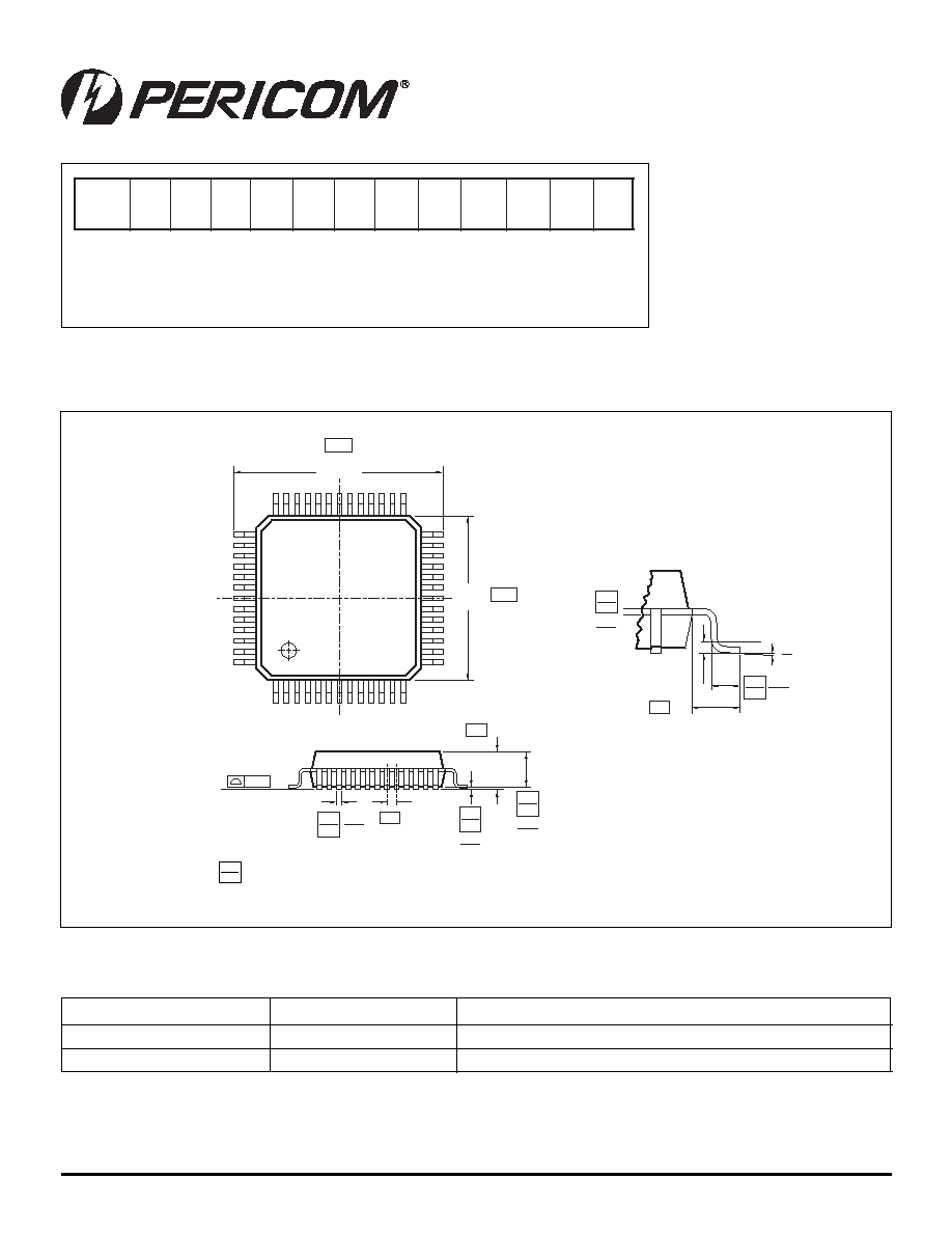
Packaging Mechanical: 52-Pin LQFP (FC)
D0≠D3 are the control bits for Qa0≠Qa3, respectively
D4≠D7 are the control bits for Qb0≠Qb3, respectively
D8≠D10 are the control bits for Qc1≠Qc3, respectively
D11 is the control bit for QSync
Freeze Data Input Protocol
t
r
a
t
S
ti
B
0
D
1
D
2
D
3
D
4
D
5
D
6
D
7
D
8
D
9
D
0
1
D
1
1
D
Seating Plane
0.65 BSC
.026
0.22
0.38
.009
.015
1.60
.063
1.35
1.45
.053
.057
0.05
0.15
.002
.006
X.XX
X.XX
DENOTES DIMENSIONS
IN MILLIMETERS
12.00 BSC
.394
Square
10.00 BSC
.472
Square
GAUGE PLANE
1.00 REF
.039
0.45
0.75
.018
.030
0.09
0.20
.004
.008
0.25 mm
Max.
0.10
.004
0
7
Notes:
1. Thermal characteristics can be found on the company web site at www.pericom.com/packaging/
Pericom Semiconductor Corporation ∑ 1-800-435-2336 ∑ www.pericom.com
Ordering Information
Ordering Code
Package Code
Package Type
PI6C2972FC
FC
52-pin LQFP
PI6C2972FCE
FC
Pb-free & Green, 52-pin LQFP