
1
PS8639 10/18/02
Product Description
PI6CV857B PLL clock device is developed for registered DDR DIMM
applications This PLL Clock Buffer is designed for 2.5 V
DDQ
and 2.5V
AV
DD
operation and differential data input and output levels.
The device is a zero delay buffer that distributes a differential clock
input pair (CLK, CLK) to ten differential pairs of clock outputs (Y[0:9],
Y[0:9]) and one differential pair feedback clock outputs
(FBOUT,FBOUT) . The clock outputs are controlled by the input
clocks (CLK, CLK), the feedback clocks (FBIN,FBIN), the 2.5V
LVCMOS input (PWRDWN) and the Analog Power input (AV
DD
).
When input PWRDWN is low while power is applied, the input
receivers are disabled, the PLL is turned off and the differential clock
outputs are 3-stated. When the AV
DD
is strapped low, the PLL is
turned off and bypassed for test purposes.
When the input frequency falls below a suggested detection fre-
quency that is below the operating frequency of the PLL, the device
will enter a low power mode. An input frequency detection circuit will
detect the low frequency condition and perform the same low power
features as when the PWRDWN input is low.
The PLL in the PI6CV857B clock driver uses the input clocks (CLK,
CLK) and the feedback clocks (FBIN,FBIN) to provide high-perfor-
mance, low-skew, low-jitter output differential clocks (Y[0:9], Y[0:9]).
The PI6CV857B is also able to track Spread Spectrum Clocking for
reduced EMI.
VD D Q
1
2
3
4
5
6
7
8
9
10
11
12
13
14
15
16
17
18
19
20
21
22
23
24
48
47
46
45
44
43
42
41
40
39
38
37
35
36
34
33
32
31
30
29
28
27
26
25
F B O U T
G N D
G N D
G N D
F B I N
F B I N
P W R D W N
G N D
G N D
Y 9
Y 8
Y 8
F B O U T
Y 7
Y 7
Y 6
Y 6
Y 5
Y 5
Y 9
G N D
G N D
G N D
Y 0
Y 0
Y 1
Y 1
VD D Q
VD D Q
VD D Q
VD D Q
VD D Q
VD D Q
VD D Q
VD D Q
G N D
C L K
C L K
Y 2
Y 2
G N D
Y 3
Y 3
Y 4
Y 4
AG N D
AV D D
Product Features
� Operating Frequency up to 200 MHz and exceeds PC2700
RDIMM specification
� Distributes one differential clock input pair to ten differential
clock output pairs.
� Inputs (CLK,CLK) and (FBIN,FBIN): SSTL_2
� Input PWRDWN: LVCMOS
� Outputs (Yx, Yx), (FBOUT, FBOUT): SSTL_2
� External feedback pins (FBIN,FBIN) are used to
synchronize the outputs to the clock input.
� Operates at AV
DD
= 2.5V for core circuit and internal PLL,
and V
DDQ
= 2.5V for differential output drivers
� Available Packages: Plastic 48-pin TSSOP
Block Diagram/Pin Configuration
PI6CV857B
1:10 PLL Clock Driver for
2.5V DDR-SDRAM Memory
12345678901234567890123456789012123456789012345678901234567890121234567890123456789012345678901212345678901234567890123456789012123456789012
12345678901234567890123456789012123456789012345678901234567890121234567890123456789012345678901212345678901234567890123456789012123456789012
Y0
Y0
Y1
PWRDWN
AVDD
FBIN
FBIN
CLK
CLK
PLL
Y1
Y2
Y2
Y3
Y3
Y4
Y4
Y5
Y5
Y6
Y6
Y7
Y7
Y8
Y8
Y9
Y9
FBOUT
FBOUT
Powerdown
and Test
Logic
48-Pin
A

2
PS8639 10/18/02
12345678901234567890123456789012123456789012345678901234567890121234567890123456789012345678901212345678901234567890123456789012123456789012
12345678901234567890123456789012123456789012345678901234567890121234567890123456789012345678901212345678901234567890123456789012123456789012
PI6CV857B
1:10 PLL Clock Driver for
2.5V DDR-SDRAM Memory
Function Table
s
t
u
p
n
I
s
t
u
p
t
u
O
L
L
P
V
A
D
D
N
W
D
R
W
P
K
L
C
K
L
C
Y
Y
T
U
O
B
F
T
U
O
B
F
D
N
G
H
L
H
L
H
L
H
f
f
o
/
d
e
s
s
a
p
y
B
D
N
G
H
H
L
H
L
H
L
f
f
o
/
d
e
s
s
a
p
y
B
X
L
L
H
Z
Z
Z
Z
f
f
o
X
L
H
L
Z
Z
Z
Z
f
f
o
)
m
o
n
(
V
5
.
2
H
L
H
L
H
L
H
n
o
)
m
o
n
(
V
5
.
2
H
H
L
H
L
H
L
n
o
)
m
o
n
(
V
5
.
2
X
z
H
M
0
2
<
)
1
(
Z
Z
Z
Z
f
f
o
Notes: For testing and power saving purposes, PI6CV857B will power down if the frequency of the reference inputs CLK, CLK is
well below the operating frequency range. The maximum power down clock frequency is below 20 MHz. For example, PI6CV857B will
be powered down when the CLK,CLK stop running.
Z = High impedance
X = Don't care
e
m
a
N
n
i
P
.
o
N
n
i
P
e
p
y
T
O
/
I
n
o
i
t
p
i
r
c
s
e
D
K
L
C
K
L
C
3
1
4
1
I
t
u
p
n
i
k
c
o
l
C
e
c
n
e
r
e
f
e
R
x
Y
6
4
,
4
4
,
9
3
,
9
2
,
7
2
,
2
2
,
0
2
,
0
1
,
5
,
3
O
.
s
t
u
p
t
u
o
k
c
o
l
C
x
Y
7
4
,
3
4
,
0
4
,
0
3
,
6
2
,
3
2
,
9
1
,
9
,
6
,
2
.
s
t
u
p
t
u
o
k
c
o
l
C
t
n
e
m
e
l
p
m
o
C
T
U
O
B
F
T
U
O
B
F
2
3
3
3
t
u
p
t
u
O
k
c
a
b
d
e
e
F
t
n
e
m
e
l
p
m
o
C
d
n
a
,t
u
p
t
u
o
k
c
a
b
d
e
e
F
N
I
B
F
N
I
B
F
6
3
5
3
I
t
u
p
n
I
k
c
a
b
d
e
e
F
t
n
e
m
e
l
p
m
o
C
d
n
a
,t
u
p
n
I
k
c
a
b
d
e
e
F
N
W
D
R
W
P
7
3
,
0
=
N
W
D
R
W
P
n
e
h
W
.
s
t
u
p
t
u
o
x
Y
d
n
a
x
Y
ll
a
r
o
f
e
l
b
a
s
i
d
t
u
p
t
u
o
d
n
a
n
w
o
d
r
e
w
o
P
a
o
t
d
e
l
b
a
s
i
d
e
r
a
s
t
u
p
t
u
o
k
c
o
l
c
l
a
it
n
e
r
e
f
fi
d
e
h
t
d
n
a
n
w
o
d
d
e
r
e
w
o
p
s
i
t
r
a
p
e
h
t
n
u
r
d
n
a
d
e
l
b
a
n
e
e
r
a
s
t
u
p
t
u
o
k
c
o
l
c
l
a
it
n
e
r
e
f
fi
d
ll
a
,
1
=
N
W
D
R
W
P
n
e
h
W
.
e
t
a
t
s
-
3
.
K
L
C
s
a
y
c
n
e
u
q
e
r
f
e
m
a
s
e
h
t
t
a
V
Q
D
D
5
4
,
8
3
,
4
3
,
8
2
,
1
2
,
5
1
,
2
1
,
1
1
,
4
r
e
w
o
P
.
O
/
I
r
o
f
y
l
p
p
u
S
r
e
w
o
P
V
A
D
D
6
1
V
A
.
y
l
p
p
u
s
r
e
w
o
p
e
r
o
c
/
g
o
l
a
n
A
D
D
g
n
it
s
e
t
r
o
f
L
L
P
e
h
t
s
s
a
p
y
b
o
t
d
e
s
u
e
b
n
a
c
V
A
n
e
h
W
.
s
e
s
o
p
r
u
p
D
D
s
i
K
L
C
d
n
a
d
e
s
s
a
p
y
b
s
i
L
L
P
,
d
n
u
o
r
g
o
t
d
e
p
p
a
r
t
s
s
i
.
s
t
u
p
t
u
o
e
c
i
v
e
d
e
h
t
o
t
y
lt
c
e
ri
d
d
e
r
e
f
f
u
b
D
N
G
A
7
1
d
n
u
o
r
G
y
r
ti
u
c
ri
c
e
r
o
c
/
g
o
l
a
n
a
e
h
t
r
o
f
e
c
n
e
r
e
f
e
r
d
n
u
o
r
g
e
h
t
s
e
d
i
v
o
r
P
.
d
n
u
o
r
g
e
r
o
c
/
g
o
l
a
n
A
D
N
G
8
4
,
2
4
,
1
4
,
1
3
,
5
2
,
4
2
,
8
1
,
8
,
7
,
1
d
n
u
o
r
G
Pinout Table
3
PS8639 10/18/02
12345678901234567890123456789012123456789012345678901234567890121234567890123456789012345678901212345678901234567890123456789012123456789012
12345678901234567890123456789012123456789012345678901234567890121234567890123456789012345678901212345678901234567890123456789012123456789012
PI6CV857B
1:10 PLL Clock Driver for
2.5V DDR-SDRAM Memory
l
o
b
m
y
S
r
e
t
e
m
a
r
a
P
.
n
i
M
.
m
o
N
.
x
a
M
s
t
i
n
U
V
A
D
D
e
g
a
tl
o
v
y
l
p
p
u
s
e
r
o
c
/
g
o
l
a
n
A
3
.
2
5
.
2
7
.
2
V
V
Q
D
D
e
g
a
tl
o
v
y
l
p
p
u
s
t
u
p
t
u
O
3
.
2
5
.
2
7
.
2
V
L
I
n
i
p
N
W
D
R
W
P
r
o
f
e
g
a
tl
o
v
t
u
p
n
i
l
e
v
e
l
-
w
o
L
3
.
0
�
7
.
0
V
H
I
n
i
p
N
W
D
R
W
P
r
o
f
e
g
a
tl
o
v
t
u
p
n
i
l
e
v
e
l
-
h
g
i
H
7
.
1
V
Q
D
D
3
.
0
+
V
I
e
g
a
tl
o
V
t
u
p
n
I
0
V
Q
D
D
I
H
O
t
n
e
r
r
u
c
t
u
p
t
u
o
l
e
v
e
l
-
h
g
i
H
�
2
1
A
m
I
L
O
t
n
e
r
r
u
c
t
u
p
t
u
o
l
e
v
e
l
-
w
o
L
�
2
1
�
V
X
I
e
g
a
tl
o
v
g
n
i
s
s
o
r
c
ri
a
p
-l
a
it
n
e
r
e
f
fi
d
t
u
p
n
I
V
(
Q
D
D
2
.
0
�
)
2
/
V
(
Q
D
D
2
.
0
+
)
2
/
V
V
X
O
t
u
p
n
i
k
c
o
l
c
M
A
R
D
e
h
t
t
a
e
g
a
tl
o
v
g
n
i
s
s
o
r
c
ri
a
p
-l
a
it
n
e
r
e
f
fi
d
t
u
p
t
u
O
V
(
Q
D
D
)
2
/
5
1
.
0
�
V
(
Q
D
D
)
2
/
5
1
.
0
+
V
N
I
l
e
v
e
l
e
g
a
tl
o
v
t
u
p
n
I
3
.
0
�
V
Q
D
D
3
.
0
+
V
D
I
K
L
C
d
n
a
K
L
C
n
e
e
w
t
e
b
e
g
a
tl
o
v
l
a
it
n
e
r
e
f
fi
d
t
u
p
n
I
6
3
.
0
V
Q
D
D
6
.
0
+
V
D
O
T
U
O
B
F
&
T
U
O
B
F
d
n
a
]
n
[
Y
&
]
n
[
Y
n
e
e
w
t
e
b
e
g
a
tl
o
v
l
a
it
n
e
r
e
f
fi
d
t
u
p
t
u
O
7
.
0
V
Q
D
D
6
.
0
+
T
A
e
r
u
t
a
r
e
p
m
e
t
ri
a
e
e
r
f
g
n
it
a
r
e
p
O
0
0
7
C
�
DC Specifications
Recommended Operating Conditions
Absolute Maximum Ratings
(Over operating free-air temperature range)
Note: Stress beyond those listed under "Absolute Maximum Ratings" may cause permanent damage to the device.
l
o
b
m
y
S
r
e
t
e
m
a
r
a
P
.
n
i
M
.
x
a
M
s
t
i
n
U
V
Q
D
D
V
A
,
D
D
e
g
n
a
r
e
g
a
tl
o
v
y
l
p
p
u
s
e
r
o
c
/
g
o
l
a
n
a
d
n
a
e
g
n
a
r
e
g
a
tl
o
v
y
l
p
p
u
s
O
/
I
5
.
0
�
6
.
3
V
V
I
e
g
n
a
r
e
g
a
tl
o
v
t
u
p
n
I
5
.
0
�
V
Q
D
D
5
.
0
+
V
O
e
g
n
a
r
e
g
a
tl
o
v
t
u
p
t
u
O
5
.
0
�
I
K
I
t
n
e
r
r
u
C
p
m
a
l
C
t
u
p
n
I
0
5
�
0
5
A
m
I
K
O
t
n
e
r
r
u
C
p
m
a
l
C
t
u
p
t
u
O
0
5
�
0
5
I
O
t
n
e
r
r
u
C
t
u
p
t
u
o
s
u
o
u
n
it
n
o
C
0
5
�
0
5
I
)
R
W
P
(
O
V
h
c
a
e
h
g
u
o
r
h
t
t
n
e
r
r
u
c
s
u
o
u
n
it
n
o
C
D
D
V
,
Q
D
D
D
N
G
r
o
,
0
0
1
�
0
0
1
g
t
s
T
e
r
u
t
a
r
e
p
m
e
t
e
g
a
r
o
t
S
5
6
�
0
5
1
o
C

4
PS8639 10/18/02
12345678901234567890123456789012123456789012345678901234567890121234567890123456789012345678901212345678901234567890123456789012123456789012
12345678901234567890123456789012123456789012345678901234567890121234567890123456789012345678901212345678901234567890123456789012123456789012
PI6CV857B
1:10 PLL Clock Driver for
2.5V DDR-SDRAM Memory
r
e
t
e
m
a
r
a
P
s
n
o
i
t
i
d
n
o
C
t
s
e
T
A
D
D
V
V
,
Q
D
D
.
n
i
M
.
p
y
T
.
x
a
M
s
t
i
n
U
V
K
I
s
t
u
p
n
i
ll
A
I
I
A
m
8
1
�
=
V
3
.
2
2
.
1
�
V
V
H
O
e
g
a
tl
o
v
t
u
p
t
u
o
h
g
i
H
I
H
O
A
�
0
0
1
�
=
V
7
.
2
o
t
3
.
2
Q
D
D
V
� 1
.
0
I
H
O
A
m
2
1
�
=
V
3
.
2
7
.
1
V
L
O
e
g
a
tl
o
v
t
u
p
t
u
o
w
o
L
I
L
O
A
�
0
0
1
=
V
7
.
2
o
t
3
.
2
1
.
0
I
L
O
A
m
2
1
=
V
3
.
2
6
.
0
I
I
N
I
B
F
,
K
L
C
V
I
V
=
Q
D
D
D
N
G
r
o
V
7
.
2
0
1
�
A
�
N
W
D
R
W
P
V
I
V
=
Q
D
D
D
N
G
r
o
I
Q
D
D
V
f
o
t
n
e
r
r
u
c
y
l
p
p
u
s
c
i
m
a
n
y
D
Q
D
D
V
D
D
V
7
.
2
=
0
0
3
A
m
t
n
e
r
r
u
c
y
l
p
p
u
s
c
it
a
t
S
r
o
z
H
M
0
2
<
K
L
C
&
K
L
C
w
o
L
=
N
W
D
R
W
P
)
4
(
0
0
1
A
�
I
D
D
A
V
A
f
o
t
n
e
r
r
u
c
y
l
p
p
u
s
c
i
m
a
n
y
D
D
D
V
D
D
V
7
.
2
=
2
1
A
m
t
n
e
r
r
u
c
y
l
p
p
u
s
c
it
a
t
S
r
o
z
H
M
0
2
<
K
L
C
&
K
L
C
w
o
L
=
N
W
D
R
W
P
)
4
(
0
0
1
A
�
C
I
K
L
C
d
n
a
K
L
C
V
I
V
=
Q
D
D
D
N
G
r
o
V
5
.
2
0
.
2
5
.
3
F
p
N
I
B
F
d
n
a
N
I
B
F
C
(
I
)
K
L
C
d
n
a
K
L
C
V
I
V
=
Q
D
D
D
N
G
r
o
V
5
.
2
�
5
2
.
0
5
2
.
0
N
I
B
F
d
n
a
N
I
B
F
C
I
e
c
n
a
ti
c
a
p
a
C
t
u
p
n
i
t
r
a
P
o
t
t
r
a
P
n
o
it
a
i
r
a
V
)
5
(
V
I
V
=
Q
D
D
D
N
G
r
o
V
5
.
2
1
Note:
4. The maximum power-down clock frequency is below 20 MHz.
5. Guaranteed by design, but not production tested.
Electrical Characteristics
Notes:
1. The PLL is able to handle spread spectrum induced skew.
2. Operating clock frequency indicates a range over which the PLL is able to lock, but in which the clock is not required to meet the
other timing parameters. (Used for low-speed debug).
3. Application clock frequency indicates a range over which the PLL meets all of the timing parameters.
Timing Requirements
(Over recommended operating free-air temperature)
l
o
b
m
y
S
n
o
i
t
p
i
r
c
s
e
D
V
A
D
D
V
,
Q
D
D
V
2
.
0
�
V
5
.
2
=
s
t
i
n
U
.
n
i
M
.
x
a
M
f
K
C
y
c
n
e
u
q
e
r
f
k
c
o
l
c
g
n
it
a
r
e
p
O
)
2
,
1
(
0
6
0
0
2
z
H
M
y
c
n
e
u
q
e
r
f
k
c
o
l
c
n
o
it
a
c
il
p
p
A
)
3
(
5
9
0
0
2
t
C
D
e
l
c
y
c
y
t
u
d
k
c
o
l
c
t
u
p
n
I
0
4
0
6
%
t
B
A
T
S
p
u
r
e
w
o
p
r
e
tf
a
e
m
it
n
o
it
a
z
il
i
b
a
t
s
L
L
P
0
0
1
s
�

5
PS8639 10/18/02
12345678901234567890123456789012123456789012345678901234567890121234567890123456789012345678901212345678901234567890123456789012123456789012
12345678901234567890123456789012123456789012345678901234567890121234567890123456789012345678901212345678901234567890123456789012123456789012
PI6CV857B
1:10 PLL Clock Driver for
2.5V DDR-SDRAM Memory
AC Specifications
Switching characteristics over recommended operating free-air temperature range (unless otherwise noted)( See Figure 1 & 2 )
r
e
t
e
m
a
r
a
P
n
o
i
t
p
i
r
c
s
e
D
m
a
r
g
a
i
D
V
A
C
C
V
,
Q
D
D
V
2
.
0
�
V
5
.
2
=
s
t
i
n
U
.
n
i
M
.
m
o
N
x
a
M
)
c
c
(
ti
jt
r
e
tt
ij
e
l
c
y
c
-
o
t
-
e
l
c
y
C
3
e
r
u
g
i
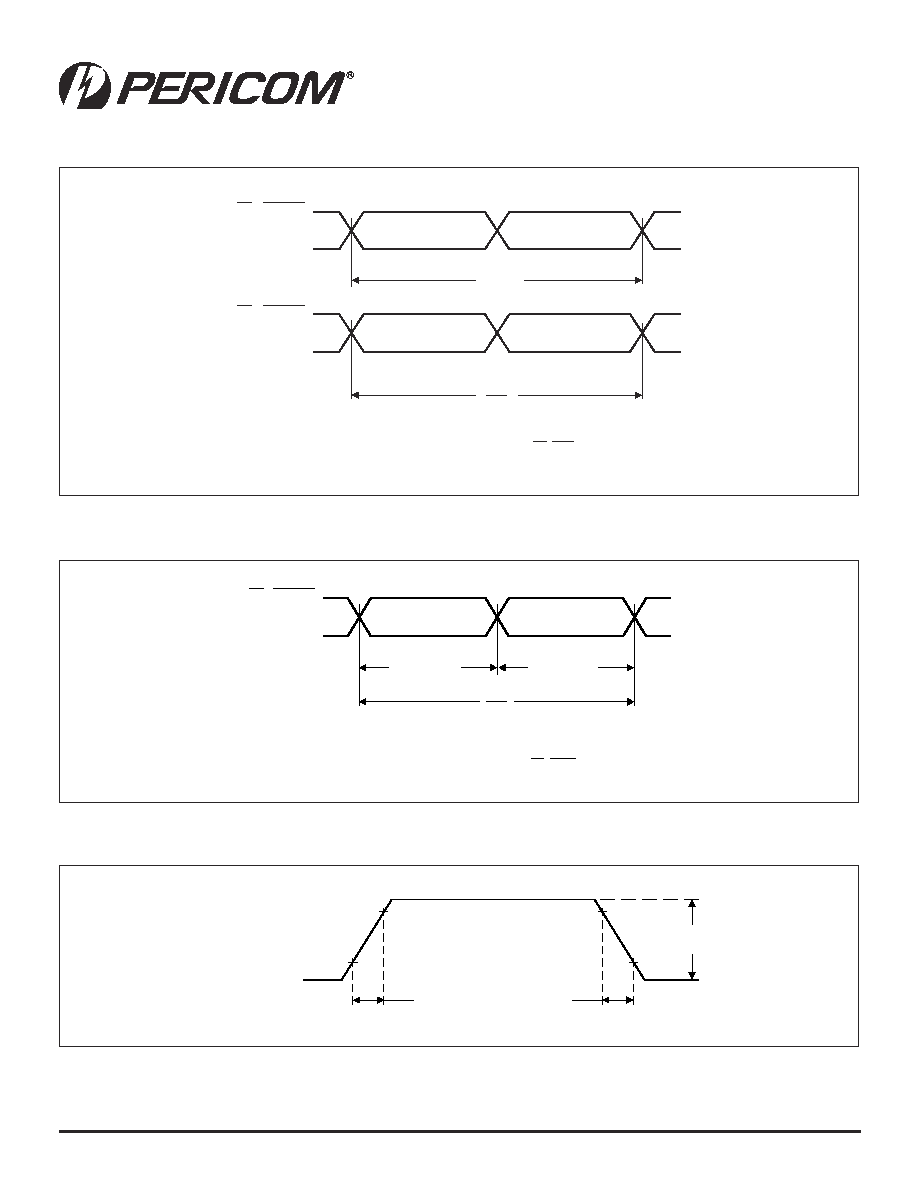
F
e
e
s
5
7
�
5
7
s
p
(
t
)
t
e
s
f
f
o
e
s
a
h
p
c
it
a
t
S
)
1
(
4
e
r
u
g
i
F
e
e
s
0
5
�
0
0
5
)
o
(
k
s
t
w
e
k
s
k
c
o
l
c
t
u
p
t
u
O
5
e
r
u
g
i
F
e
e
s
0
0
1
)
r
e
p
(
ti
jt
r
e
tt
ij
d
o
i
r
e
P
6
e
r
u
g
i
F
e
e
s
5
7
�
5
7
)
r
e
p
h
(
ti
jt
r
e
tt
ij
d
o
i
r
e
p
-
fl
a
H
7
e
r
u
g
i
F
e
e
s
0
0
1
�
0
0
1
)i
(l
s
t
e
t
a
r
w
e
l
s
k
c
o
l
c
t
u
p
n
I
)
2
(
8
e
r
u
g
i
F
e
e
s
0
.
1
0
.
4
s
n
/
V
)
o
(l
s
t
e
t
a
r
w
e
l
s
k
c
o
l
c
t
u
p
t
u
O
)
2
(
8
e
r
u
g
i
F
e
e
s
0
.
1
0
.
2
g
n
i
w
o
ll
o
f
e
h
t
h
ti
w
s
r
e
z
i
s
e
h
t
n
y
s
C
S
S
g
n
it
r
o
p
p
u
s
e
li
h
w
s
r
e
t
e
m
a
r
a
p
e
v
o
b
a
e
h
t
ll
a
g
n
it
e
e
m
f
o
e
l
b
a
p
a
c
s
i
L
7
5
8
V
C
6
I
P
e
h
t
n
o
L
L
P
e
h
T
s
r
e
t
e
m
a
r
a
p
)
3
(
.
y
c
n
e
u
q
e
r
f
n
o
it
a
l
u
d
o
m
C
S
S
0
0
.
0
3
0
0
.
0
5
z
H
k
n
o
it
a
i
v
e
d
y
c
n
e
u
q
e
r
f
t
u
p
n
i
k
c
o
l
c
C
S
S
0
0
.
0
0
5
.
0
�
%
h
t
d
i
w
d
n
a
b
p
o
o
l
L
L
P
2
z
H
M
e
l
g
n
a
e
s
a
h
P
1
3
0
.
0
�
s
e
e
r
g
e
d
Notes:
1. Static Phase offset does not include Jitter.
2. The slew rate is determined from the IBIS model with test load shown in Figure1.
3. The SSC requirements meet the Intel PC100 SDRAM Registered DIMM specification.

6
PS8639 10/18/02
12345678901234567890123456789012123456789012345678901234567890121234567890123456789012345678901212345678901234567890123456789012123456789012
12345678901234567890123456789012123456789012345678901234567890121234567890123456789012345678901212345678901234567890123456789012123456789012
PI6CV857B
1:10 PLL Clock Driver for
2.5V DDR-SDRAM Memory
Figure 2. Output Load Test Circuit
Figure 1. IBIS Model Output Load
�VDDQ/2
VDDQ/2
Z=60
C=14pF
R=120
Z=60
GND
GND
R=1M
PROBE
PI6CV857L
R=1M
C=14pF
C=1pF
C=1pF
V
DD
PI6CV857
R=60
V
CLK
R=60
V
CLK
V
DD
/2

7
PS8639 10/18/02
12345678901234567890123456789012123456789012345678901234567890121234567890123456789012345678901212345678901234567890123456789012123456789012
12345678901234567890123456789012123456789012345678901234567890121234567890123456789012345678901212345678901234567890123456789012123456789012
PI6CV857B
1:10 PLL Clock Driver for
2.5V DDR-SDRAM Memory
Figure 3. Cycle-to-Cycle Jitter
Figure 4. Static Phase Offset
Figure 5. Output Skew
F B I N
F B I N
C K
C K
t
( )
n
t
( )
n+1
t
=
1
n = N
t
( ) n
N
(N is a large number of samples)
t
jit(cc)
=
t
cycle n
-
t
cycle n+1
t
cycle n+1
t
cycle n
Y x , F B O U T
Y x , F B O U T
t
sk(o)
Y x
Y x
Y x , F B O U T
Y x , F B O U T
8
PS8639 10/18/02
12345678901234567890123456789012123456789012345678901234567890121234567890123456789012345678901212345678901234567890123456789012123456789012
12345678901234567890123456789012123456789012345678901234567890121234567890123456789012345678901212345678901234567890123456789012123456789012
PI6CV857B
1:10 PLL Clock Driver for
2.5V DDR-SDRAM Memory
Figure 6. Period Jitter
Figure 7. Half-Period Jitter
Figure 8. Input and Output Slew Rates
Clock Inputs
and Outputs
V
ID
t
sl(i),
t
sl(o)
8 0 %
2 0 %
t
sl(i),
t
sl(o)
8 0 %
2 0 %
Y x , F B O U T
Y x , F B O U T
Y x , F B O U T
Y x , F B O U T
t
cycle n
f
O
1
t
jit(per)
=
t
cycle n
f
O
1
Yx, FBOUT
Yx, FBOUT
t
half period n
t
n+1
half period
f
O
1
t
jit(hper)
=
t
half period n
2*f
O
1

9
PS8639 10/18/02
12345678901234567890123456789012123456789012345678901234567890121234567890123456789012345678901212345678901234567890123456789012123456789012
12345678901234567890123456789012123456789012345678901234567890121234567890123456789012345678901212345678901234567890123456789012123456789012
PI6CV857B
1:10 PLL Clock Driver for
2.5V DDR-SDRAM Memory
Pericom Semiconductor Corporation
2380 Bering Drive � San Jose, CA 95131 � 1-800-435-2336 � Fax (408) 435-1100 � http://www.pericom.com
Packaging Mechanical: 48-Pin TSSOP
.236
.244
.488
.496
.002
.006
SEATING PLANE
.007
.010
.0197
BSC
.004
.008
.319
1
48
12.4
12.6
6.0
6.2
0.50
0.17
0.27
8.1
0.05
0.15
0.09
0.20
X.XX
X.XX
DENOTES DIMENSIONS
IN MILLIMETERS
.018
.030
0.45
0.75
.047
1.20 Max
BSC
e
d
o
C
g
n
i
r
e
d
r
O
e
m
a
N
e
g
a
k
c
a
P
e
p
y
T
e
g
a
k
c
a
P
A
B
7
5
8
V
C
6
I
P
8
4
A
P
O
S
S
T
e
d
i
w
li
m
-
0
4
2
,
n
i
p
-
8
4
Ordering Information