1
PS8312 08/04/98
12345678901234567890123456789012123456789012345678901234567890121234567890123456789012345678901212345678901234567890123456789012123456789012
12345678901234567890123456789012123456789012345678901234567890121234567890123456789012345678901212345678901234567890123456789012123456789012
PI74ALVCH16863
18-Bit Transceiver with 3-State Outputs
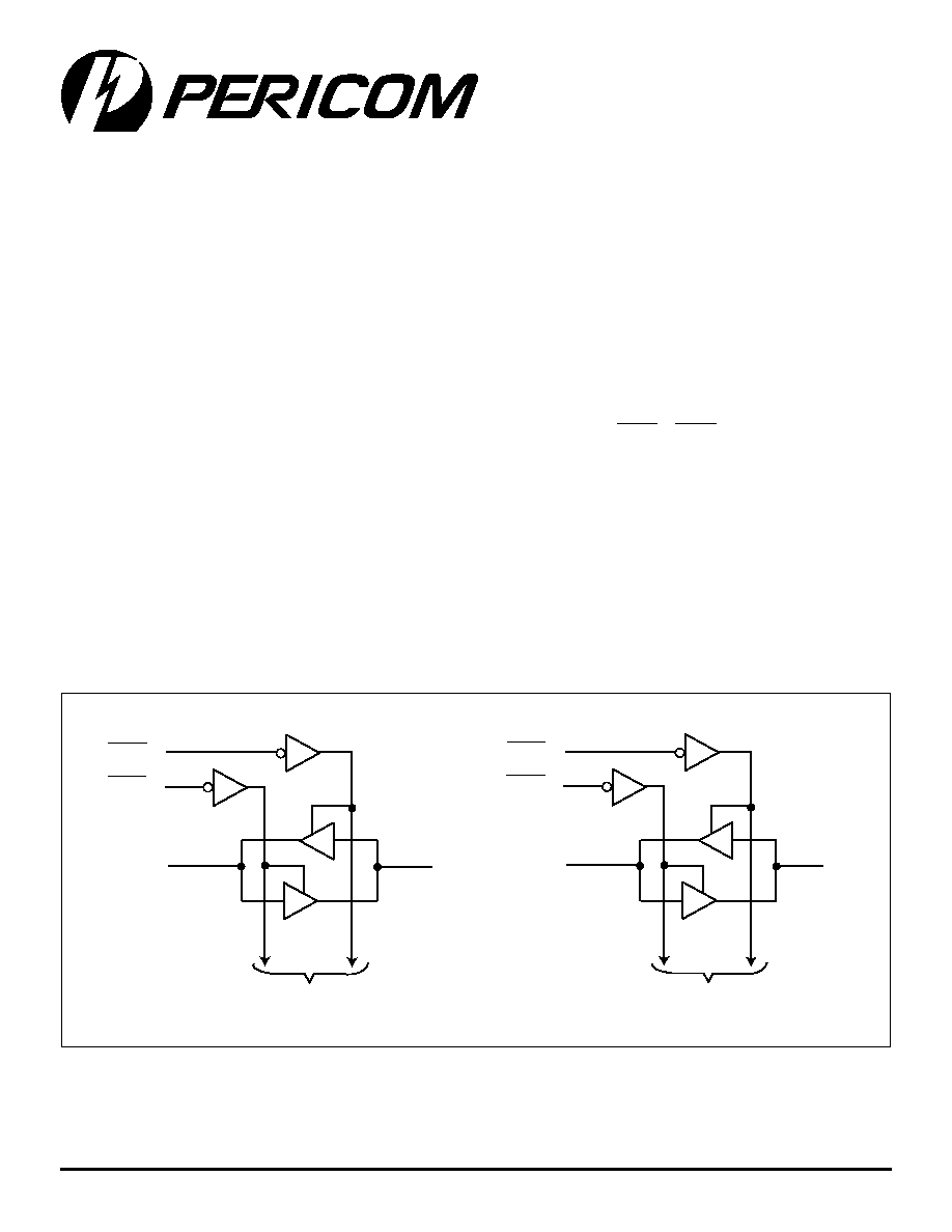
Logic Block Diagram
Product Description
Pericom Semiconductors PI74ALVCH series of logic circuits are
produced in the Companys advanced 0.5 micron CMOS technology,
achieving industry leading speed.
The PI74ALVCH16863 is an 18-bit noninverting transceiver designed
for synchronous communication between data buses. The control-
function implementation minimizes external timing requirements.
The PI74ALCH16863 can be used as two 9-bit transceivers or one 18-
bit transceiver.They allow data transmission from the A bus to the
B bus or from the B bus to the A bus, depending on the logic level
at the output-enable (OEAB or OEBA) inputs.
To ensure the high-impedance state during power up or power down,
OE should be tied to Vcc through a pull-up resistor; the minimum
value of the resistor is determined by the current-sinking capability
of the driver.
The PI74ALVCH16863 has Bus Hold which retains the data
inputs last state whenever the data input goes to high-impedance
preventing floating inputs and eliminating the need for pullup/
down resistors.
Product Features
� PI74ALVCH16863 is designed for low voltage operation
� V
CC
= 2.3V to 3.6V
� Hysteresis on all inputs
� Typical V
OLP
(Output Ground Bounce)
< 0.8V at V
CC
= 3.3V, T
A
= 25�C
� Typical V
OHV
(Output V
OH
Undershoot)
< 2.0V at V
CC
= 3.3V, T
A
= 25�C
� Bus Hold retains last active bus state during 3-State,
eliminating the need for external pullup resistors
� Industrial operation at 40�C to +85�C
� Packages available:
56-pin 240 mil wide plastic TSSOP (A)
56-pin 300 mil wide plastic SSOP (V)
1OEBA
1OEAB
1A1
55
1B1
2
1
56
2OEBA
2OEAB
2A1
41
2B1
16
28
29
To Eight Other Channels
To Eight Other Channels

PI74ALVCH16863
18-Bit Transceiver with 3-State Outputs
2
PS8312 08/04/98
12345678901234567890123456789012123456789012345678901234567890121234567890123456789012345678901212345678901234567890123456789012123456789012
Pin Name
Description
OExx
Output Enable Input (Active LOW)
Ax
Data I/O
Bx
Data I/O
GND
Ground
V
CC
Power
1
2
3
4
5
6
7
8
9
10
11
12
13
14
15
16
17
18
19
20
21
22
23
24
56
55
54
53
52
51
50
49
48
47
46
45
44
43
42
41
40
39
38
37
36
35
34
33
25
26
27
28
32
31
30
29
Product Pin Description
Truth Table
(1)
Note:
1. H = High Signal Level
L = Low Signal Level
Z = High Impedance
= LOW-to-HIGH Transition
Product Pin Configuration
56-Pin
A, V
1OEAB
1B1
1B2
GND
1B3
1B4
VCC
1B5
1B6
1B7
GND
1B8
1B9
GND
GND
2B1
2B2
GND
2B3
2B4
2B5
VCC
2B6
2B7
GND
2B8
2B9
2OEAB
1OEBA
1A1
1A2
GND
1A3
1A4
VCC
1A5
1A6
1A7
GND
1A8
1A9
GND
GND
2A1
2A2
GND
2A3
2A4
2A5
VCC
2A6
2A7
GND
2A8
2A9
2OEBA
s
t
u
p
n
I
B
t
u
p
t
u
O
B
A
E
O
A
B
E
O
H
L
s
u
b
A
o
t
a
t
a
d
B
L
H
s
u
b
B
o
t
a
t
a
d
A
H
H
e
c
n
a
d
e
p
m
I
h
g
i
H

PI74ALVCH16863
18-Bit Transceiver with 3-State Outputs
3
PS8312 08/04/98
12345678901234567890123456789012123456789012345678901234567890121234567890123456789012345678901212345678901234567890123456789012123456789012
Note:
1. Unused control inputs must be held HIGH or LOW to prevent them from floating.
Recommended Operating Conditions
(1)
s
r
e
t
e
m
a
r
a
P
n
o
it
p
i
r
c
s
e
D
s
n
o
it
i
d
n
o
C
t
s
e
T
.
n
i
M
.
p
y
T
.
x
a
M
s
ti
n
U
V
C
C
e
g
a
tl
o
V
y
l
p
p
u
S
3
.
2
6
.
3
V
V
H
I
e
g
a
tl
o
V
H
G
I
H
t
u
p
n
I
V
C
C
V
7
.
2
o
t
V
3
.
2
=
7
.
1
V
C
C
V
6
.
3
o
t
V
7
.
2
=
0
.
2
V
L
I
e
g
a
tl
o
V
W
O
L
t
u
p
n
I
V
C
C
V
7
.
2
o
t
V
3
.
2
=
7
.
0
V
C
C
V
6
.
3
o
t
V
7
.
2
=
8
.
0
V
N
I
e
g
a
tl
o
V
t
u
p
n
I
0
V
C
C
V
T
U
O
e
g
a
tl
o
V
t
u
p
t
u
O
0
V
C
C
I
H
O
t
n
e
rr
u
C
t
u
p
t
u
O
l
e
v
el
-
h
g
i
H
V
C
C
V
3
.
2
=
2
1
-
A
m
V
C
C
V
7
.
2
=
2
1
-
V
C
C
V
0
.
3
=
4
2
-
I
L
O
t
n
e
rr
u
C
t
u
p
t
u
O
l
e
v
el
-
w
o
L
V
C
C
V
3
.
2
=
2
1
V
C
C
V
7
.
2
=
2
1
V
C
C
V
0
.
3
=
4
2
T
A
e
r
u
t
a
r
e
p
m
e
T
ri
A
-
e
e
r
F
g
n
it
a
r
e
p
O
0
4
-
5
8
C
�
D /tDv
ll
a
F
r
o
e
si
R
n
o
it
i
s
n
a
r
T
t
u
p
n
I
0
0
1
V
/
s
n
Storage Temperature ................................................. 65�C to +150�C
Ambient Temperature with Power Applied ................. 40�C to +85�C
Input Voltage Range, V
IN ............................................
0.5V to V
CC
+0.5V
Output Voltage Range, V
OUT .....................................
0.5V to V
CC
+0.5V
DC Input Voltage .......................................................... 0.5V to +5.0V
DC Output Current ...................................................................100 mA
Power Dissipation ........................................................................ 1.0W
Note:
Stresses greater than those listed under MAXIMUM
RATINGS may cause permanent damage to the device.
This is a stress rating only and functional operation of the
device at these or any other conditions above those
indicated in the operational sections of this specification
is not implied. Exposure to absolute maximum rating
conditions for extended periods may affect reliability.
Maximum Ratings
(Above which the useful life may be impaired. For user guidelines, not tested.)

PI74ALVCH16863
18-Bit Transceiver with 3-State Outputs
4
PS8312 08/04/98
12345678901234567890123456789012123456789012345678901234567890121234567890123456789012345678901212345678901234567890123456789012123456789012
DC Electrical Characteristics
(Over the Operating Range, T
A
= 40�C to +85�C, V
CC
= 3.3V � 10%)
s
r
e
t
e
m
a
r
a
P
s
n
o
it
i
d
n
o
C
t
s
e
T
V
C
C
)
1
(
.
n
i
M
.
p
y
T
)
2
(
.
x
a
M
s
ti
n
U
V
H
O
I
H
O
0
0
1
-
=
mA
.
x
a
M
o
t
.
n
i
M
V
C
C
- 2
.
0
V
I
H
O
A
M
6
-
=
V
H
I
=
V
7
.
1
V
3
.
2
0
.
2
I
H
O
2
1
-
=
mA
V
H
I
=
V
7
.
1
V
3
.
2
7
.
1
V
H
I
=
V
0
.
2
7
.
2 V
2
.
2
V
H
I
=
V
0
.
2
V
0
.
3
4
.
2
I
H
O
A
M
4
2
-
=
V
H
I
V
0
.
2
=
V
0
.
3
0
.
2
V
L
O
I
L
O
0
0
1
=
mA
.
x
a
M
o
t
.
n
i
M
2
.
0
V
I
L
O
=
A
m
6
V
L
I
=
V
7
.
0
V
3
.
2
4
.
0
I
L
O
A
M
2
1
=
V
L
I
=
V
7
.
0
V
3
.
2
7
.
0
V
L
I
=
V
8
.
0
V
7
.
2
4
.
0
I
L
O
=
A
m
4
2
V
L
I
=
V
8
.
0
V
0
.
3
5
5
.
0
I
I
V
I
= V
CC
D
N
G
r
o
V
6
.
3
5
�
mA
I
I
)
d
l
o
H
(
)
3
(
V
I
=
V
7
.
0
V
3
.
2
5
4
V
I
=
V
7
.
1
5
4
-
V
I
=
V
8
.
0
V
0
.
3
5
7
V
I
=
V
0
.
2
5
7
-
V
I
=
V
6
.
3
o
t
0
V
6
.
3
0
0
5
�
I
Z
O
)
4
(
V
O
= V
C
C
D
N
G
r
o
V
6
.
3
0
1
�
I
C
C
V
I
= V
C
C
D
N
G
r
o
I
O
0
=
V
6
.
3
0
4
DI
C
C
V
t
a
t
u
p
n
i
e
n
O
C
C
,
V
6
.
0
-
V
t
a
st
u
p
n
i
r
e
h
t
O
C
C
D
N
G
r
o
V
6
.
3
o
t
V
3
0
5
7
C
I
st
u
p
n
I
l
o
rt
n
o
C
V
I
= V
C
C
D
N
G
r
o
V
3
.
3
5
.
3
F
p
st
u
p
n
I
a
t
a
D
6
C
O
I
st
r
o
p
B
r
o
A
V
O
= V
C
C
D
N
G
r
o
V
3
.
3
5
.
7
F
p
Notes:
1. For Max. or Min. conditions, use appropriate value specified under Electrical Characteristics for the applicable device type.
2. Typical values are at V
CC
= 3.3V, +25�C ambient and maximum loading.
3. Bus Hold maximum dynamic current required to switch the input from one state to another.
4. For I/O ports, the I
OZ
includes the input leakage current.

PI74ALVCH16863
18-Bit Transceiver with 3-State Outputs
5
PS8312 08/04/98
12345678901234567890123456789012123456789012345678901234567890121234567890123456789012345678901212345678901234567890123456789012123456789012
Pericom Semiconductor Corporation
2380 Bering Drive � San Jose, CA 95131 � 1-800-435-2336 � Fax (408) 435-1100 � http://www.pericom.com
Switching Characteristics Over Operating Range
(1)
Notes:
1. See test circuit and waveforms.
2. Minimum limits are guaranteed but not tested on Propagation Delays.
s
r
e
t
e
m
a
r
a
P
m
o
r
F
)t
u
p
n
I
(
o
T
)t
u
p
t
u
O
(
V
C
C
V
2
.
0
�
V
5
.
2
=
V
C
C
V
7
.
2
=
V
C
C
V
.
0
�
V
3
.
3
=
s
ti
n
U
.
n
i
M
)
2
(
.
x
a
M
.
n
i
M
)
2
(
.
x
a
M
.
n
i
M
)
2
(
.
x
a
M
t
D
P
B
r
o
A
A
r
o
B
0
.
1
1
.
4
4
1
4
.
3
s
n
t
N
E
r
o
B
A
E
O
A
B
E
O
B
r
o
A
0
.
1
7
.
5
8
.
5
0
.
1
7
.
4
t
S
I
D
r
o
B
A
E
O
A
B
E
O
B
r
o
A
3
.
1
5
.
5
7
.
4
4
.
1
2
.
4
Operating Characteristics, T
A
= 25�C
r
e
t
e
m
a
r
a
P
s
n
o
it
i
d
n
o
C
t
s
e
T
V
C
C
V
2
.
0
�
V
5
.
2
=
V
C
C
V
3
.
0
�
V
3
.
3
=
s
ti
n
U
l
a
c
i
p
y
T
C
D
P
n
o
it
a
p
i
s
si
D
r
e
w
o
P
e
c
n
a
ti
c
a
p
a
C
d
el
b
a
n
E
st
u
p
t
u
O
C
L
,
F
p
0
5
=
z
H
M
0
1
=
f
1
2
0
3
F
p
d
el
b
a
si
D
st
u
p
t
u
O
2
3