1
PXXXX 11/07/00
ADVANCE INFORMATION
Product Description
Pericom Semiconductors PI74AVC+ series of logic circuits are
produced using the Companys advanced submicron CMOS
technology, achieving industry leading speed.
The PI74AVC+16373 is particularly suited for implementing buffer
registers, I/O ports, bidirectional bus drivers, and working registers.
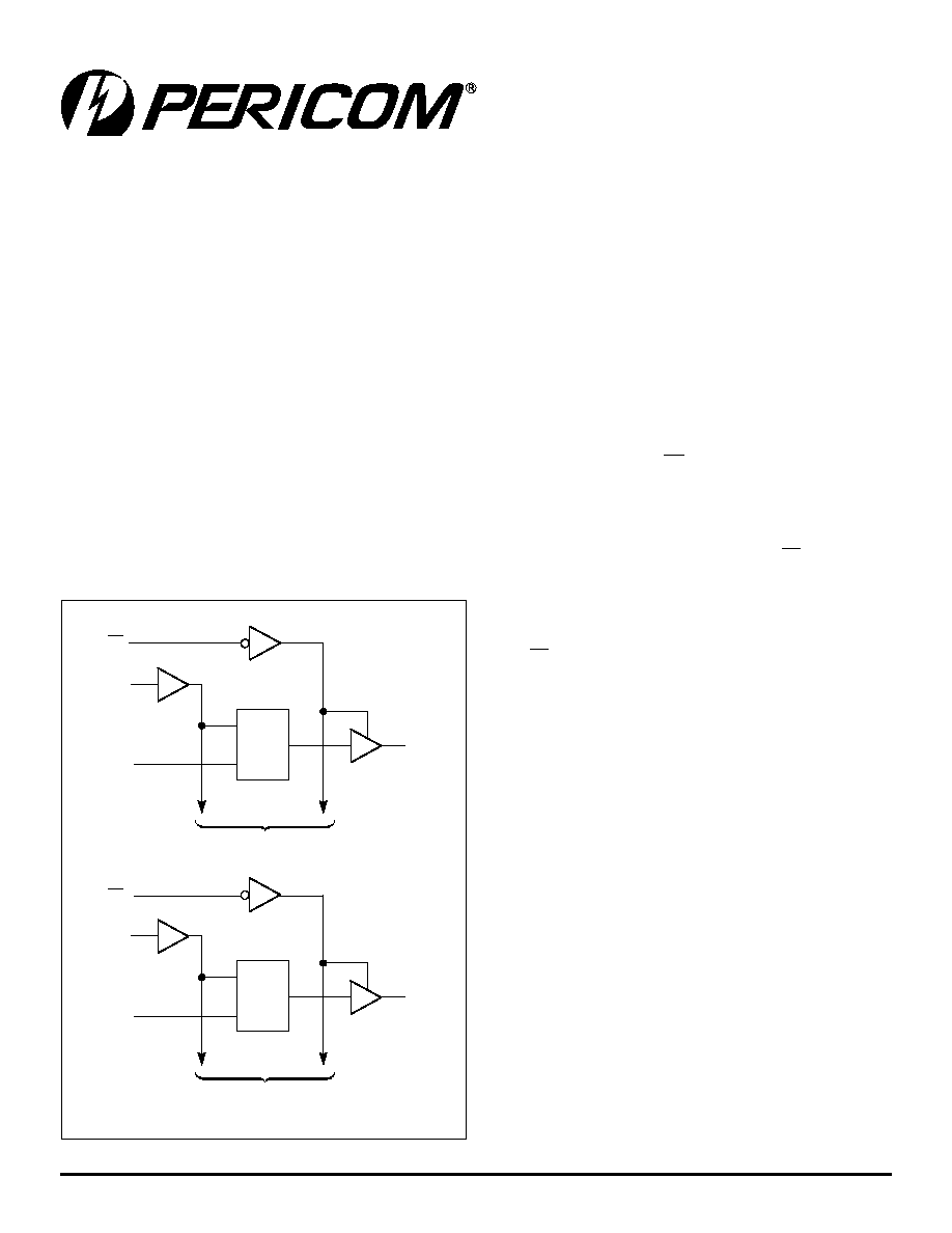
This device can be used as two 8-bit latches or one 16-bit latch.
When the Latch Enable (LE) input is HIGH, the Q outputs follow the
(D) inputs. When LE is taken LOW, the Q outputs are latched at the
levels set up at the D inputs.
A buffered Output Enable (OE) input can be used to place the
eight outputs in either a normal logic state (high or low logic
levels) or a high-impedance state in which the outputs neither
load nor drive the bus lines significantly. The high-impedance state
and the increased drive provide the capability to drive bus lines
without need for interface or pullup components. OE does not affect
internal operations of the latch. Old data can be retained
or new data can be entered while the outputs are in the high
impedance state.
To ensure the high impedance state during power up or power
down, OE should be tied to V
CC
through a pullup resistor; the
minimum value of the resistor is determined by the current-sinking
capability of the driver.
12345678901234567890123456789012123456789012345678901234567890121234567890123456789012345678901212345678901234567890123456789012123456789012
12345678901234567890123456789012123456789012345678901234567890121234567890123456789012345678901212345678901234567890123456789012123456789012
12345678901234567890123456789012123456789012345678901234567890121234567890123456789012345678901212345678901234567890123456789012123456789012
2.5V 16-Bit Transparent D-Type Latch
with 3-State Outputs
Logic Block Diagram
Product Features
PI74AVC+16373 is designed for low voltage operation,
V
CC
= 1.65V to 3.6V
True �24mA Balanced Drive @ 3.3V
Compatible with Philips and T.I. AVC Logic family
I
OFF
supports partial power-down operation
3.6V I/O Tolerant inputs and outputs
All outputs contain a patented DDC (Dynamic Drive
Control) circuit that reduces noise without degrading
propagation delay.
Industrial operation at 40�C to +85�C
Available Packages:
48-pin 240-mil wide plastic TSSOP
48-pin 173-mil wide plastic TVSOP
PI74AVC+16373
ADVANCE INFORMATION
1LE
1Q1
1D
C1
1D1
To Seven Other Channels
1OE
1
48
47
2
2LE
2Q1
1D
C1
2D1
To Seven Other Channels
25
36
13
24
2OE
ADVANCE INFORMATION
PI74AVC+16373
2.5V 16-Bit Transparent D-Type Latch
with 3-State Outputs
2
PXXXX 11/07/00
12345678901234567890123456789012123456789012345678901234567890121234567890123456789012345678901212345678901234567890123456789012123456789012
12345678901234567890123456789012123456789012345678901234567890121234567890123456789012345678901212345678901234567890123456789012123456789012
Maximum Ratings
(Above which the useful life may be impaired. For user guidelines, not tested.)
Supply voltage range, V
CC
............................................. 0.5V to +4.6V
Input voltage range, V
I
................................................... 0.5V to +4.6V
Voltage range applied to any output in the
high-impedance or power-off state, V
O
(1)
...................... 0.5V to +4.6V
Voltage range applied to any output in the
high or low state, V
O
(1,2)
......................................... 0.5V to V
CC
+0.5V
Input clamp current, I
IK
(V
I
<0) .................................................... 50mA
Output clamp current, I
OK
(V
O
<0) .............................................. 50mA
Continuous output current, I
O
.................................................... �50mA
Continuous current through each V
CC
or GND ......................... �100mA
Package thermal impedance,
JA
(3)
: package A .........................64�C/W
package K ..........................48�C/W
Storage Temperature range, T
stg
.................................... 65�C to 150�C
1. Input & output negative-voltage ratings may be
exceeded if the input and output curent rating are
observed.
2. Output positive-voltage rating may be exceeded up to
4.6V maximum if the output current rating is observed.
3. The package thermal impedance is calculated in accor-
dance with JESD 51.
Notes:
Stresses greater than those listed under MAXIMUM
RATINGS may cause permanent damage to the device.
This is a stress rating only and functional operation of the
device at these or any other conditions above those
indicated in the operational sections of this specification
is not implied. Exposure to absolute maximum rating
conditions for extended periods may affect reliability.
s
t
u
p
n
I
s
t
u
p
t
u
O
E
O
E
L
D
Q
L
H
H
H
L
H
L
L
L
L
X
Q
0
H
X
X
Z
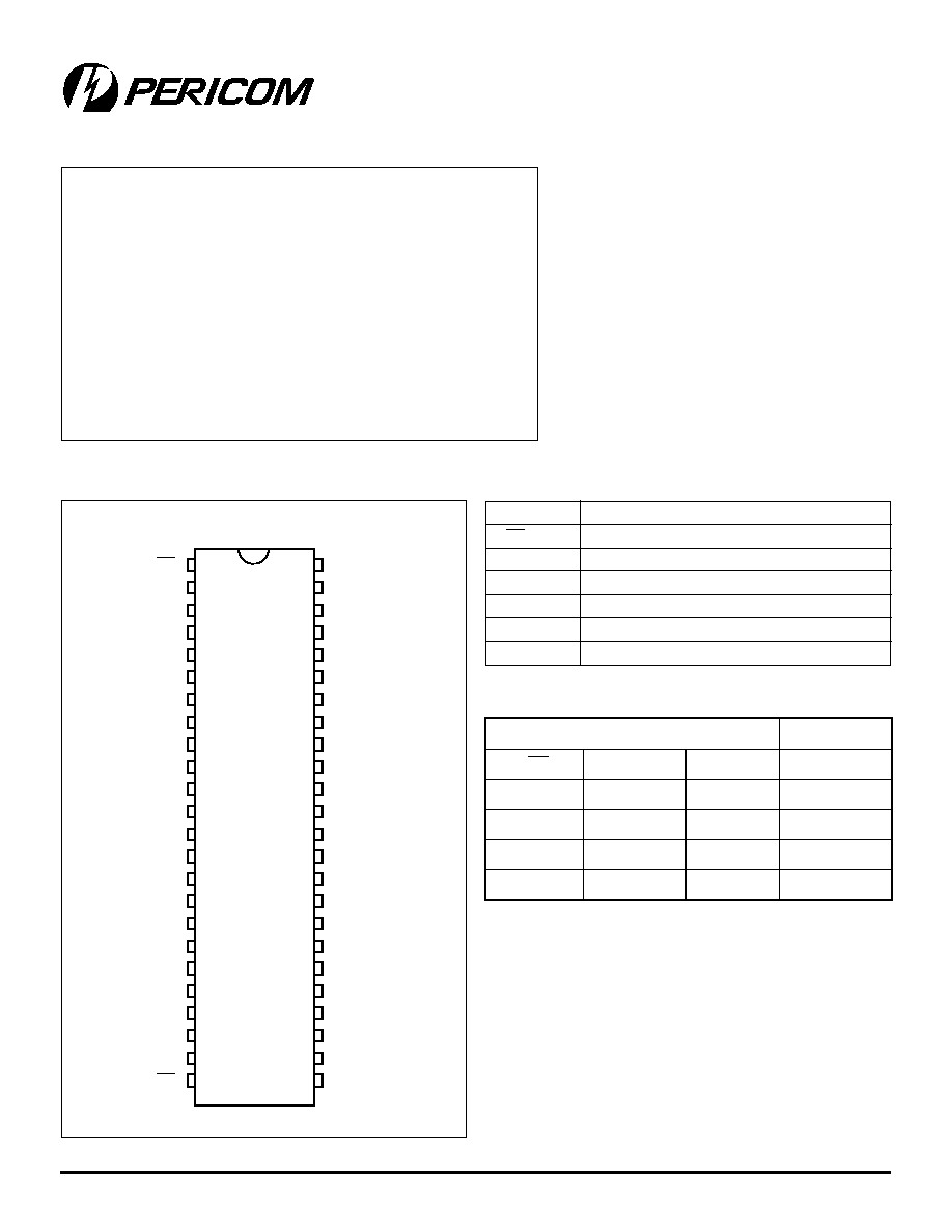
Pin Name
Description
OE
3-State Output Enable Inputs (Active LOW)
LE
Latch Enable (Active HIGH)
Dx
Data Inputs
Qx
3-State Outputs
GND
Ground
V
CC
Power
Product Pin Description
Truth Table
(1)
Product Pin Configuration
Notes:
1. H = High Signal Level
L = Low Signal Level
X = Don't Care or Irrelevant
Z = High Impedance
1
2
3
4
5
6
7
8
9
48
10
47
11
46
12
45
13
44
14
43
15
42
16
41
17
40
18
39
19
38
20
37
21
36
22
35
23
34
24
33
32
31
30
29
28
27
26
25
1OE
1LE
1Q1
1D1
1Q2
1D2
GND
GND
1Q3
1D3
1Q4
1D4
V
1Q5
1D5
1Q6
1D6
GND
GND
1Q7
1D7
1Q8
1D8
2Q1
2D1
2Q2
2D2
GND
GND
2Q3
2D3
2Q4
2D4
2Q5
2D5
2Q6
2D6
GND
GND
2Q7
2D7
2Q8
2D8
2OE
2LE
CC
VCC
VCC
VCC
48-Pin
A,K

3
PXXXX 11/07/00
12345678901234567890123456789012123456789012345678901234567890121234567890123456789012345678901212345678901234567890123456789012123456789012
12345678901234567890123456789012123456789012345678901234567890121234567890123456789012345678901212345678901234567890123456789012123456789012
ADVANCE INFORMATION
PI74AVC+16373
2.5V 16-Bit Transparent D-Type Latch
with 3-State Outputs
Recommended Operating Conditions
(1)
.
n
i
M
.
x
a
M
s
ti
n
U
V
C
C
e
g
a
tl
o
V
y
l
p
p
u
S
g
n
it
a
r
e
p
O
4
.
1
6
.
3
V
y
l
n
o
n
o
it
n
e
t
e
r
a
t
a
D
2
.
1
V
H
I
e
g
a
tl
o
V
t
u
p
n
I
l
e
v
el
-
h
g
i
H
V
C
C
V
2
.
1
=
V
C
C
V
C
C
V
6
.
1
o
t
V
4
.
1
=
V
x
5
6
.
0
C
C
V
C
C
V
5
9
.
1
o
t
V
5
6
.
1
=
V
x
5
6
.
0
C
C
V
C
C
V
7
.
2
o
t
V
3
.
2
=
7
.
1
V
C
C
V
6
.
3
o
t
V
3
=
2
V
L
I
e
g
a
tl
o
V
t
u
p
n
I
l
e
v
el
-
w
o
L
V
C
C
V
2
.
1
=
D
N
G
V
C
C
V
6
.
1
o
t
V
4
.
1
=
V
x
5
3
.
0
C
C
V
C
C
V
5
9
.
1
o
t
V
5
6
.
1
=
V
x
5
3
.
0
C
C
V
C
C
V
7
.
2
o
t
V
3
.
2
=
7
.
0
V
C
C
V
6
.
3
o
t
V
3
=
8
.
0
V
I
e
g
a
tl
o
V
t
u
p
n
I
0
6
.
3
V
O
e
g
a
tl
o
V
t
u
p
t
u
O
e
t
a
t
S
e
v
it
c
A
0
V
C
C
e
t
a
t
S
-
3
0
6
.
3
I
S
H
O
t
n
e
rr
u
c
t
u
p
t
u
o
l
e
v
el
-
h
g
i
H
V
C
C
V
6
.
1
o
t
V
4
.
1
=
4
A
m
V
C
C
V
5
9
.
1
o
t
V
5
6
.
1
=
6
V
C
C
V
7
.
2
o
t
V
3
.
2
=
2
1
V
C
C
V
6
.
3
o
t
V
3
=
4
2
I
S
L
O
t
n
e
rr
u
c
t
u
p
t
u
o
l
e
v
el
-
w
o
L
V
C
C
V
6
.
1
o
t
V
4
.
1
=
4
V
C
C
V
5
9
.
1
o
t
V
5
6
.
1
=
6
V
C
C
V
7
.
2
o
t
V
3
.
2
=
2
1
V
C
C
V
6
.
3
o
t
V
3
=
4
2
t
e
t
a
r
ll
a
f
r
o
e
si
r
n
o
it
i
s
n
a
rt
t
u
p
n
I
v
V
C
C
V
6
.
3
o
t
V
4
.
1
=
5
V
/
s
n
T
A
e
r
u
t
a
r
e
p
m
e
t
ri
a
-
e
e
rf
g
n
it
a
r
e
p
O
0
4
5
8
C
�
Notes:
1. All unused inputs must be held at V
CC
or GND to ensure proper device operation.

ADVANCE INFORMATION
PI74AVC+16373
2.5V 16-Bit Transparent D-Type Latch
with 3-State Outputs
4
PXXXX 11/07/00
12345678901234567890123456789012123456789012345678901234567890121234567890123456789012345678901212345678901234567890123456789012123456789012
12345678901234567890123456789012123456789012345678901234567890121234567890123456789012345678901212345678901234567890123456789012123456789012
s
r
e
t
e
m
a
r
a
P
s
n
o
it
i
d
n
o
C
t
s
e
T
)
1
(
V
C
C
.
n
i
M
.
p
y
T
.
x
a
M
s
ti
n
U
V
H
O
I
H
O
0
0
1
=
�A
V
6
.
3
o
t
V
4
.
1
V
C
C
V
2
.
0
V
I
S
H
O
4
=
m
V
A
H
I
V
1
9
.
0
=
V
4
.
1
5
0
.
1
I
S
H
O
6
=
m
V
A
H
I
V
7
0
.
1
=
V
5
6
.
1
2
.
1
I
S
H
O
2
1
=
m
V
A
H
I
V
7
.
1
=
V
3
.
2
5
7
.
1
I
S
H
O
4
2
=
m
V
A
H
I
V
2
=
V
3
0
.
2
V
L
O
I
S
L
O
0
0
1
=
�A
V
6
.
3
o
t
V
4
.
1
2
.
0
I
S
L
O
4
= m
V
A
L
I
V
9
4
.
0
=
V
4
.
1
4
.
0
I
S
L
O
6
= m
V
A
L
I
V
7
5
.
0
=
V
5
6
.
1
5
4
.
0
I
S
L
O
2
1
=
m
V
A
L
I
V
7
.
0
=
V
3
.
2
5
5
.
0
I
S
L
O
4
2
=
m
V
A
L
I
V
8
.
0
=
V
3
5
7
.
0
I
I
st
u
p
n
I
l
o
rt
n
o
C
V
I
V
=
C
C
D
N
G
r
o
V
6
.
3
5
.
2
�
A
�
I
F
F
O
V
I
V
r
o
O
V
6
.
3
=
0
0
1
�
I
Z
O
V
O
V
=
C
C
D
N
G
r
o
V
6
.
3
0
1
�
I
C
C
V
I
V
=
C
C
I
D
N
G
r
o
O
0
=
V
6
.
3
0
4
C
I
st
u
p
n
I
l
o
rt
n
o
C
V
I
V
=
C
C
D
N
G
r
o
V
5
.
2
5
.
3
F
p
V
3
.
3
5
.
3
st
u
p
n
I
a
t
a
D
V
5
.
2
6
V
3
.
3
6
C
O
st
u
p
t
u
O
V
O
V
=
C
C
D
N
G
r
o
V
5
.
2
5
.
6
V
3
.
3
5
.
6
Note: Typical values are measured at T
A
= 25�C.
DC Electrical Characteristics (Over the Operating Range, T
A
= -40�C +85�C)

5
PXXXX 11/07/00
12345678901234567890123456789012123456789012345678901234567890121234567890123456789012345678901212345678901234567890123456789012123456789012
12345678901234567890123456789012123456789012345678901234567890121234567890123456789012345678901212345678901234567890123456789012123456789012
ADVANCE INFORMATION
PI74AVC+16373
2.5V 16-Bit Transparent D-Type Latch
with 3-State Outputs
Switching Characteristics over recommended operating free-air temperature range
(unless otherwise noted, see Figures 1 thru 4)
Operating Characteristics, T
A
= 25�C
s
r
e
t
e
m
a
r
a
P
s
n
o
it
i
d
n
o
C
t
s
e
T
V
C
C
V
8
.
1
=
V
5
1
.
0
�
V
C
C
V
5
.
2
=
V
2
.
0
�
V
C
C
V
3
.
3
=
V
3
.
0
�
s
ti
n
U
l
a
c
i
p
y
T
l
a
c
i
p
y
T
l
a
c
i
p
y
T
n
o
it
a
p
i
s
si
D
r
e
w
o
P
d
p
C
e
c
n
a
ti
c
a
p
a
C
d
el
b
a
n
E
st
u
p
t
u
O
C
L
,
F
p
0
=
z
H
M
0
1
=
f
0
4
3
4
7
4
F
p
d
el
b
a
si
D
st
u
p
t
u
O
0
2
2
2
4
2
s
r
e
t
e
m
a
r
a
P
m
o
r
F
)t
u
p
n
I
(
o
T
)t
u
p
t
u
O
(
V
C
C
V
2
.
1
=
V
C
C
V
5
.
1
=
V
1
.
0
�
V
C
C
V
8
.
1
=
V
5
1
.
0
�
V
C
C
V
5
.
2
=
V
2
.
0
�
V
C
C
V
3
.
3
=
V
3
.
0
�
s
ti
n
U
.
p
y
T
.
n
i
M
.
x
a
M
.
n
i
M
.
x
a
M
.
n
i
M
.
x
a
M
.
n
i
M
.
x
a
M
t
d
p
D
Q
8
.
5
2
.
1
8
.
6
1
7
.
5
8
.
0
3
.
3
7
.
0
8
.
2
s
n
E
L
2
.
7
4
.
1
3
.
8
1
.
1
6
.
6
8
.
0
4
7
.
0
2
.
3
t
n
e
E
O
Q
4
.
7
6
.
1
8
.
8
6
.
1
7
.
6
4
.
1
3
.
4
7
.
0
4
.
3
t
si
d
E
O
Q
4
.
8
5
.
2
4
.
9
3
.
2
8
.
7
3
.
1
2
.
4
2
.
1
9
.
3
V
C
C
V
2
.
1
=
V
C
C
V
5
.
1
=
V
1
.
0
�
V
C
C
V
8
.
1
=
V
5
1
.
0
�
V
C
C
V
5
.
2
=
V
2
.
0
�
V
C
C
V
3
.
3
=
V
3
.
0
�
s
ti
n
U
.
n
i
M
.
x
a
M
.
n
i
M
.
x
a
M
.
n
i
M
.
x
a
M
.
n
i
M
.
x
a
M
.
n
i
M
.
x
a
M
t
w
H
G
I
H
E
L
,
n
o
it
a
r
u
d
e
sl
u
P
2
.
2
2
8
.
1
s
n
t
u
s
E
L
e
r
o
f
e
b
a
t
a
d
,
e
m
it
p
u
t
e
S
7
.
1
2
.
1
1
.
1
9
.
0
8
.
0
t
h
E
L
r
e
tf
a
a
t
a
d
,
e
m
it
d
l
o
H
2
1
.
1
1
.
1
1
.
1
1
Timing requirements over recommended operating free-air temperature range
(unless otherwise noted, see Figures 1 thru 4)