1
PS2088B 09/19/02
12345678901234567890123456789012123456789012345678901234567890121234567890123456789012345678901212345678901234567890123456789012123456789012
12345678901234567890123456789012123456789012345678901234567890121234567890123456789012345678901212345678901234567890123456789012123456789012
12345678901234567890123456789012123456789012345678901234567890121234567890123456789012345678901212345678901234567890123456789012123456789012
PI74LCX16245
Fast CMOS 3.3V 16-Bit
Bidirectional Transceiver
Product Features
∑ Functionally compatible with FCT3, LVT, and
74 series 16245 families of products
∑ Tri-State outputs
∑ 5V Tolerant inputs and outputs
∑ 2.0V-3.6V V
CC
supply operation
∑ Balanced sink and source output drives (24mA)
∑ Low ground bounce outputs
∑ Power down High Impedance inputs and outputs
∑ Supports live insertion
∑ ESD Protection exceeds 2000V, Human Body Model
200V, Machine Model
∑ Packages available:
≠ 48-pin 240-mil wide plastic TSSOP (A)
≠ 48-pin 300-mil wide plastic SSOP (V)
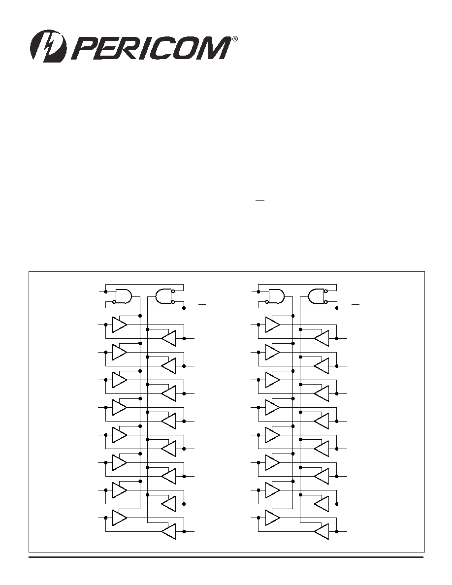
Logic Block Diagram
Product Description
Pericom Semiconductor's PI74LCX series of logic circuits are
produced in the Company's advanced 0.6 micron CMOS technology,
achieving industry leading speed grades.
The PI74LCX16245 is a 16-bit bidirectional transceiver designed for
asynchronous two-way communication between data buses. The
direction control input pin (xDIR) determines the direction of data
flow through the bidirectional transceiver. The Direction and Output
Enable controls are designed to operate this device as either two
independent 8-bit transceivers or one 16-bit transceiver. The output
enable (OE) input, when HIGH, disables both A and B ports by
placing them in HIGH Z condition.
The PI74LCX16245 can be driven from either 3.3V or 5.0V devices
allowing this device to be used as a translator in a mixed
3.3/5.0V system.
1
B
0
1
A
0
1
OE
1DIR
2DIR
1
B
1
1
A
1
1
B
2
1
A
2
1
B
3
A
31
1
B
4
1
A
4
1
B
5
1
A
5
1
B
6
1
A
6
1
B
7
1
A
7
2
B
0
2
A
0
2OE
2
B
1
2
A
1
2
B
2
2
A
2
2
B
3
2
A
3
2
B
4
2
A
4
2
B
5
2
A
5
2
B
6
2
A
6
2
B
7
2
A
7
2
PS2088B 09/19/02
12345678901234567890123456789012123456789012345678901234567890121234567890123456789012345678901212345678901234567890123456789012123456789012
12345678901234567890123456789012123456789012345678901234567890121234567890123456789012345678901212345678901234567890123456789012123456789012
PI74LCX16245
3.3V 16-Bit Bidirectional Transceiver
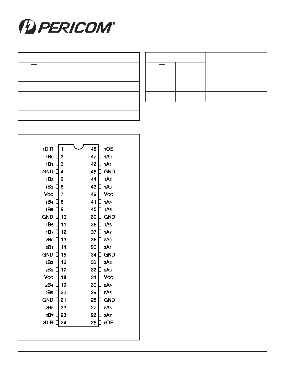
Product Pin Description
Truth Table
(1)
Note:
1. H = High Voltage Level
X = Don't Care,
L = Low Voltage Level
Z = High Impedance
e
m
a
N
n
i
P
n
o
i
t
p
i
r
c
s
e
D
O
x E
)
W
O
L
e
v
it
c
A
(
s
t
u
p
n
I
e
l
b
a
n
E
t
u
p
t
u
O
e
t
a
t
S
-
3
R
I
D
x
t
u
p
n
I
l
o
r
t
n
o
C
n
o
it
c
e
ri
D
X
A
X
s
t
u
p
n
I
e
t
a
t
S
-
3
r
o
s
t
u
p
n
I
A
e
d
i
S
X
B
X
s
t
u
p
t
u
O
e
t
a
t
S
-
3
r
o
s
t
u
p
t
u
O
B
e
d
i
S
D
N
G
d
n
u
o
r
G
V
C
C
r
e
w
o
P
s
t
u
p
n
I
)
1
(
s
t
u
p
t
u
O
)
1
(
E
O
x
R
I
D
x
L
L
A
s
u
B
o
t
a
t
a
D
B
s
u
B
L
H
B
s
u
B
o
t
a
t
a
D
A
s
u
B
H
X
Z
Product Pin Configuration
48-Pin
A, V
3
PS2088B 09/19/02
12345678901234567890123456789012123456789012345678901234567890121234567890123456789012345678901212345678901234567890123456789012123456789012
12345678901234567890123456789012123456789012345678901234567890121234567890123456789012345678901212345678901234567890123456789012123456789012
PI74LCX16245
3.3V 16-Bit Bidirectional Transceiver
Maximum Ratings
(Above which the useful life may be impaired. For user guidelines, not tested.)
Note:
Stresses greater than those listed under MAXIMUM
RATINGS may cause permanent damage to the device.
This is a stress rating only and functional operation of
the device at these or any other conditions above those
indicated in the operational sections of this specifica-
tion is not implied. Exposure to absolute maximum rating
conditions for extended periods may affect reliability.
l
o
b
m
y
S
r
e
t
e
m
a
r
a
P
.
n
i
M
.
x
a
M
s
t
i
n
U
V
C
C
e
g
a
tl
o
V
y
l
p
p
u
S
g
n
it
a
r
e
p
O
0
.
2
6
.
3
V
n
o
it
n
e
t
e
R
a
t
a
D
5
.
1
6
.
3
V
I
e
g
a
tl
o
V
t
u
p
n
I
0
5
.
5
V
O
e
g
a
tl
o
V
t
u
p
t
u
O
e
t
a
t
S
W
O
L
r
o
H
G
I
H
0
V
CC
e
t
a
t
S
-
3
0
5
.
5
I
H
O
I
/
L
O
t
n
e
r
r
u
C
t
u
p
t
u
O
V
C
C
=
V
6
.
3
-
V
0
.
3
4
2
±
A
m
V
C
C
=
V
7
.
2
2
1
±
T
A
e
r
u
t
a
r
e
p
m
e
T
g
n
it
a
r
e
p
O
ri
A
-
e
e
r
F
-
0
4
5
8
+
∞
C
/t
V
e
t
a
R
e
g
d
E
t
u
p
n
I
V
,
V
0
.
2
-
V
8
.
0
=
V
C
C
V
0
.
3
=
0
0
1
V
/
s
n
Recommended Operating Conditions
Storage Temperature ............................................................ ≠65∞C to +150∞C
Ambient Temperature with Power Applied ............................ ≠40∞C to +85∞C
Supply Voltage to Ground Potential (Inputs & Vcc Only) ...... ≠0.5V to +7.0V
Supply Voltage to Ground Potential (Outputs & D/O Only) ... ≠0.5V to +7.0V
DC Input Voltage .................................................................... ≠0.5V to +7.0V
DC Output Current .............................................................................. 120mA
Power Dissipation .................................................................................. 1.0W

4
PS2088B 09/19/02
12345678901234567890123456789012123456789012345678901234567890121234567890123456789012345678901212345678901234567890123456789012123456789012
12345678901234567890123456789012123456789012345678901234567890121234567890123456789012345678901212345678901234567890123456789012123456789012
PI74LCX16245
3.3V 16-Bit Bidirectional Transceiver
Notes:
1. For Max. or Min. conditions, use appropriate value specified under Electrical Characteristics for the applicable device type.
2. Typical values are at V
CC
= 3.3V, +25∞C ambient.
3. Per TTL driven input; all other inputs at V
CC
or GND.
s
r
e
t
e
m
a
r
a
P
n
o
i
t
p
i
r
c
s
e
D
s
n
o
i
t
i
d
n
o
C
t
s
e
T
)
1
(
.
n
i
M
p
y
T
)
2
(
.
x
a
M
s
t
i
n
U
V
H
I
e
g
a
tl
o
V
H
G
I
H
t
u
p
n
I
l
e
v
e
L
H
G
I
H
c
i
g
o
L
d
e
e
t
n
a
r
a
u
G
0
.
2
--
--
V
V
L
I
e
g
a
tl
o
V
W
O
L
t
u
p
n
I
l
e
v
e
L
W
O
L
c
i
g
o
L
d
e
e
t
n
a
r
a
u
G
--
--
8
.
0
V
H
O
e
g
a
tl
o
V
H
G
I
H
t
u
p
t
u
O
V
C
C
6
.
3
-
7
.
2
=
I
H
O
A
m
1
.
0
≠
=
V
CC
2
.
0
-
--
--
V
C
C
7
.
2
=
I
H
O
A
m
2
1
≠
=
2
.
2
--
--
V
C
C
0
.
3
=
I
H
O
A
m
8
1
≠
=
4
.
2
--
--
I
H
O
A
m
4
2
≠
=
2
.
2
--
--
V
L
O
e
g
a
tl
o
V
W
O
L
t
u
p
t
u
O
V
C
C
6
.
3
-
7
.
2
=
I
L
O
A
m
1
.
0
=
--
--
2
.
0
V
C
C
7
.
2
=
I
L
O
A
m
2
1
=
--
--
4
.
0
V
C
C
0
.
3
=
I
L
O
A
m
6
1
=
--
--
4
.
0
I
L
O
A
m
4
2
=
--
--
5
5
.
0
V
K
I
e
g
a
tl
o
V
e
d
o
i
D
p
m
a
l
C
V
C
C
,.
n
i
M
=
I
N
I
A
m
8
1
≠
=
--
-
7
.
0
-
2
.
1
I
I
t
n
e
r
r
u
C
e
g
a
k
a
e
L
t
u
p
n
I
0
V
I
V
5
.
5
V
C
C
6
.
3
-
7
.
2
=
--
--
5
±
A
µ
I
Z
O
e
g
a
k
a
e
L
t
u
p
t
u
O
e
t
a
t
S
-
3
0
V
O
V
5
.
5
V
I
V
=
H
I
V
r
o
L
I
V
C
C
6
.
3
-
7
.
2
=
--
--
5
±
I
F
F
O
e
l
b
a
s
i
D
n
w
o
D
r
e
w
o
P
V
C
C
,
V
0
=
V
N
I
V
r
o
T
U
O
V
5
.
5
--
--
0
1
±
I
C
C
t
n
e
r
r
u
C
y
l
p
p
u
S
r
e
w
o
P
t
n
e
c
s
e
i
u
Q
V
C
C
.
x
a
M
=
V
N
I
V
r
o
D
N
G
=
C
C
1
.
0
0
1
I
C
C
t
n
e
r
r
u
C
y
l
p
p
u
S
r
e
w
o
P
t
n
e
c
s
e
i
u
Q
H
G
I
H
s
t
u
p
n
I
L
T
T
V
C
C
.
x
a
M
=
V
N
I
V
=
C
C
V
6
.
0
≠
)
3
(
0
0
5
s
r
e
t
e
m
a
r
a
P
n
o
i
t
p
i
r
c
s
e
D
s
n
o
i
t
i
d
n
o
C
t
s
e
T
.
p
y
T
s
t
i
n
U
C
N
I
e
c
n
a
ti
c
a
p
a
C
t
u
p
n
I
V
C
C
V
,
n
e
p
O
=
I
V
r
o
V
0
=
C
C
7
F
p
C
T
U
O
e
c
n
a
ti
c
a
p
a
C
t
u
p
t
u
O
V
C
C
V
,
V
3
.
3
=
I
V
r
o
V
0
=
C
C
8
C
D
P
e
c
n
a
ti
c
a
p
a
C
n
o
it
a
p
i
s
s
i
D
r
e
w
o
P
V
C
C
V
,
V
3
.
3
=
I
V
r
o
V
0
=
C
C
,
z
H
M
0
1
=
F
0
2
Capacitance
DC Electrical Characteristics
(Over the Operating Range, T
A
= -40∞C to +85∞C, V
CC
= 2.7V to 3.6V)

5
PS2088B 09/19/02
12345678901234567890123456789012123456789012345678901234567890121234567890123456789012345678901212345678901234567890123456789012123456789012
12345678901234567890123456789012123456789012345678901234567890121234567890123456789012345678901212345678901234567890123456789012123456789012
PI74LCX16245
3.3V 16-Bit Bidirectional Transceiver
Switching Characteristics over Operating Range
Notes:
1. Skew between any two outputs, of the same package, switching in the same direction.
Dynamic Switching Characteristics
(T
A
= +25∞C)
Note:
1. Measured with n≠1 outputs switching from High-to-Low or Low-to-High. The remaining output is measured in the LOW state.
s
r
e
t
e
m
a
r
a
P
n
o
i
t
p
i
r
c
s
e
D
s
n
o
i
t
i
d
n
o
C
V
CC
V
3
.
0
±
V
3
.
3
=
V
CC
V
7
.
2
=
s
t
i
n
U
.
n
i
M
.
x
a
M
.
n
i
M
.
x
a
M
t
H
L
P
t
L
H
P
y
a
l
e
D
n
o
it
a
g
a
p
o
r
P
D
XX
O
o
t
XX
C
L
F
p
0
5
=
R
L
0
0
5
=
5
.
1
5
.
4
5
.
1
2
.
5
s
n
t
H
Z
P
t
L
Z
P
e
m
it
e
l
b
a
n
E
t
u
p
t
u
O
5
.
1
5
.
6
5
.
1
2
.
7
t
Z
H
P
t
Z
L
P
e
m
i
T
e
l
b
a
s
i
D
t
u
p
t
u
O
5
.
1
4
.
6
5
.
1
9
.
6
t
)
O
(
K
S
w
e
k
S
t
u
p
t
u
O
)
1
(
0
.
1
s
r
e
t
e
m
a
r
a
P
n
o
i
t
p
i
r
c
s
e
D
s
n
o
i
t
i
d
n
o
C
t
s
e
T
)
1
(
.
p
y
T
s
t
i
n
U
V
P
L
O
e
g
a
tl
o
V
k
a
e
P
W
O
L
c
i
m
a
n
y
D
V
C
C
C
,
V
3
.
3
=
L
F
p
0
5
=
V
H
I
V
,
V
3
.
3
=
L
I
V
0
=
8
.
0
V
V
V
L
O
e
g
a
tl
o
V
y
e
ll
a
V
W
O
L
c
i
m
a
n
y
D
6
PS2088B 09/19/02
12345678901234567890123456789012123456789012345678901234567890121234567890123456789012345678901212345678901234567890123456789012123456789012
12345678901234567890123456789012123456789012345678901234567890121234567890123456789012345678901212345678901234567890123456789012123456789012
PI74LCX16245
3.3V 16-Bit Bidirectional Transceiver
Pericom Semiconductor Corporation
2380 Bering Drive ∑ San Jose, CA 95131 ∑ 1-800-435-2336 ∑ Fax (408) 435-1100 ∑ http://www.pericom.com
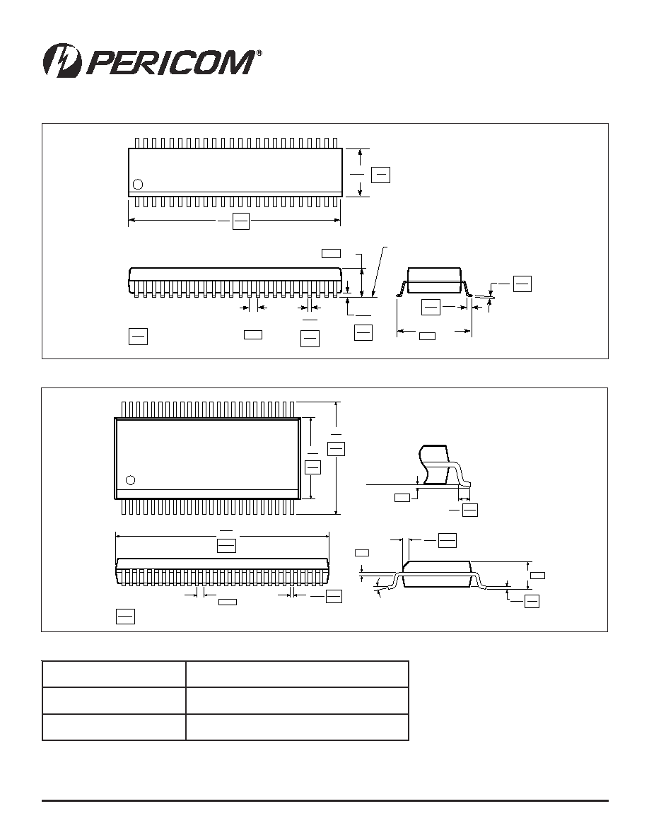
Packaging Mechanical: 48-Pin TSSOP (A) Package
Packaging Mechanical: 48-Pin SSOP (V) Package
.236
.244
.488
.496
.002
.006
SEATING PLANE
.007
.010
.0197
BSC
.004
.008
.319
1
48
12.4
12.6
6.0
6.2
0.50
0.17
0.27
8.1
0.05
0.15
0.09
0.20
X.XX
X.XX
DENOTES DIMENSIONS
IN MILLIMETERS
.018
.030
0.45
0.75
.047
1.20 Max
BSC
0.20
0.51
1.01
0.25
0.381
0.635
.008
.008
.016
0-8∞
0.20
0.40
.110 2.79
.010
Gauge Plane
.02
.04
.015
.025
x 45∞
.025 BSC
0.635
.291
.299
X.XX
X.XX
DENOTES DIMENSIONS
IN MILLIMETERS
7.39
7.59
.395
.420
10.03
10.67
.620
.630
15.75
16.00
.008
.0135
0.20
0.34
1
48
Nom.
Max
Ordering Information
e
d
o
C
g
n
i
r
e
d
r
O
n
o
i
t
p
i
r
c
s
e
D
A
5
4
2
6
1
X
C
L
4
7
I
P
)
A
(
P
O
S
S
T
c
i
t
s
a
l
P
e
d
i
w
li
m
-
0
4
2
n
i
P
-
8
4
V
5
4
2
6
1
X
C
L
4
7
I
P
)
V
(
P
O
S
S
c
i
t
s
a
l
P
e
d
i
w
li
m
-
0
0
3
n
i
P
-
8
4