
1
PS8691 07/01/03
Product Description
Pericom Semiconductor's PI74LVTC series of logic circuits are
produced using the Company's advanced CMOS technology,
achieving industry leading speed.
The PI74LVTC244 is a non-inverting 8-bit buffer and line driver
designed for low-voltage 2.7V to 3.6V V
CC
operation, with the
capability of interfacing to the 5V system environment. With its
balanced drive characteristics, this high-speed, low power device
provides low ground bounce and transmission line impedance
matching. This makes it ideal for driving on board buses and
transmission lines. The device can be used as two 4-bit buffers with
separate output enable (OE) inputs.
When V
CC
is between 0 to 1.5V during power up or power down, the
outputs of the device are in the high-impedance state. To ensure
the high-impedance state above 1.5V, OE should be tied to Vcc
through a pullup resistor; the minimum value of the resistor is
determined by the current sinking capability of the driver.
The device fully supports live-insertion with its I
off
and power-up/
down 3-state. The I
off
circuitry disables the outputs when the
power is off, preventing the backflow of damaging current through
the device. Power-up/down 3-state places the outputs in the
high-impedance state during power up or power down, preventing
driver conflict.
12345678901234567890123456789012123456789012345678901234567890121234567890123456789012345678901212345678901234567890123456789012123456789012
12345678901234567890123456789012123456789012345678901234567890121234567890123456789012345678901212345678901234567890123456789012123456789012
12345678901234567890123456789012123456789012345678901234567890121234567890123456789012345678901212345678901234567890123456789012123456789012
3.3V 8-Bit Buffers/Line Drivers
with 3-State Outputs
Logic Block Diagram
Product Features
∑
Advanced low power CMOS design for 2.7V to 3.6V
V
CC
operation
∑
Supports 5V input/output tolerance in mixed signal mode
operation
∑
Function compatible with LVT family of products
∑
Balanced ±24mA output drive
∑
Typical V
OLP
(Output Ground Bounce) <0.8V at V
CC
=3.3V,
T
A
=25∞C
∑
I
off
and Power Up/Down 3-State support live insertion
∑
Latch-up performance exceeds 200mA Per JESD78
∑
ESD protection exceeds JESD 22
- 2000V Human-Body Model (A114-B)
- 200V Machine Model (A115-A)
∑
Packages (Pb-free available):
- 20-pin 209-mil wide plastic SSOP (H20)
- 20-pin 173-mil wide plastic TSSOP (L20)
- 20-pin 300-mil wide plastic SOIC (S20)
PI74LVTC244
1OE
1A1
1Y1
1A2
1Y2
1A3
1Y3
1A4
1Y4
2OE
2A1
2Y1
2A2
2Y2
2A3
2Y3
2A4
2Y4
8
6
4
2
1
12
14
16
18
17
15
13
11
19
3
5
7
9

2
PS8691 07/01/03
PI74LVTC244
3.3V 8-Bit Buffers/Line Drivers
with 3-State Outputs
12345678901234567890123456789012123456789012345678901234567890121234567890123456789012345678901212345678901234567890123456789012123456789012
12345678901234567890123456789012123456789012345678901234567890121234567890123456789012345678901212345678901234567890123456789012123456789012
Maximum Ratings
(Above which the useful life may be impaired.
For user guidelines, not tested.)
Supply voltage range, V
CC
.............................. ≠0.5V to +6.5V
Input voltage range, V
I
(1)
................................ ≠0.5V to +6.5V
Voltage range applied to any output in the
high-impedance or power-off state, V
O
(1)
....... ≠0.5V to +6.5V
Voltage range applied to any output in the
active state, V
O
(1), (2)
................................ ≠0.5V to V
CC
+0.5V
Input clamp current, I
IK
(V
I
<0) ..................................... ≠50mA
Output clamp current, I
OK
(V
O
<0) ............................... ≠50mA
Continous Output Current I
O
....................................... ±50mA
Continous Current through each V
CC
or GND pin ............... ±100mA
Package thermal impedance,
JA
(3)
: package H ........... 81∞C/W
package L ............ 84∞C/W
package S ............ 84∞C/W
Storage Temperature range, T
stg
..................... ≠65∞C to 150∞C
1. Input negative-voltage and output voltage ratings may be exceeded if the
input and output clamp current ratings are observed.
2. This value is limited to 6.5V maximum.
3. The package thermal impedance is calculated in accordance with JESD 51.
Notes:
Stresses greater than those listed under MAXIMUM RATINGS may
cause permanent damage to the device. This is a stress rating only and
functional operation of the device at these or any other conditions above
those indicated in the operational sections of this specification is not
implied. Exposure to absolute maximum rating conditions for extended
periods may affect reliability.
s
t
u
p
n
I
s
t
u
p
t
u
O
E
O
x
x
A
x
x
Y
x
L
H
H
L
L
L
H
X
Z
Product Pin Description
Truth Table
(4)
Product Pin Configuration
Notes:
4. H = High Signal Level
L = Low Signal Level
X = Don't Care or Irrelevant
Z = High Impedance
e
m
a
N
n
i
P
n
o
i
t
p
i
r
c
s
e
D
E
O
x
)
W
O
L
e
v
it
c
A
(
s
t
u
p
n
I
e
l
b
a
n
E
t
u
p
t
u
O
e
t
a
t
S
-
3
x
A
x
s
t
u
p
n
I
x
Y
x
s
t
u
p
t
u
O
e
t
a
t
S
-
3
D
N
G
d
n
u
o
r
G
V
C
C
r
e
w
o
P
1
2
3
4
5
6
7
8
9
20
10
19
18
17
16
15
14
13
12
11
1OE
1A1
2Y4
1A2
GND
2Y2
2Y3
1A3
1A4
2Y1
VCC
2OE
1Y1
2A4
2A1
1Y3
1Y2
2A3
2A2
1Y4
20-Pin
H, L, S

PI74LVTC244
3.3V 8-Bit Buffers/Line Drivers
with 3-State Outputs
3
PS8691 07/01/03
12345678901234567890123456789012123456789012345678901234567890121234567890123456789012345678901212345678901234567890123456789012123456789012
12345678901234567890123456789012123456789012345678901234567890121234567890123456789012345678901212345678901234567890123456789012123456789012
Recommended Operating Conditions
(5)
.
n
i
M
.
x
a
M
s
t
i
n
U
V
C
C
e
g
a
tl
o
V
y
l
p
p
u
S
g
n
it
a
r
e
p
O
7
.
2
6
.
3
V
V
H
I
e
g
a
tl
o
V
t
u
p
n
I
l
e
v
e
l
-
h
g
i
H
V
C
C
V
6
.
3
o
t
V
7
.
2
=
0
.
2
V
L
I
e
g
a
tl
o
V
t
u
p
n
I
l
e
v
e
l
-
w
o
L
V
C
C
V
6
.
3
o
t
V
7
.
2
=
8
.
0
V
I
e
g
a
tl
o
V
t
u
p
n
I
0
5
.
5
V
O
e
g
a
tl
o
V
t
u
p
t
u
O
e
t
a
t
S
w
o
L
r
o
h
g
i
H
0
V
C
C
e
t
a
t
S
-
3
0
5
.
5
I
H
O
t
n
e
r
r
u
c
t
u
p
t
u
o
l
e
v
e
l
-
h
g
i
H
V
C
C
V
7
.
2
=
2
1
≠
A
m
V
C
C
V
6
.
3
o
t
V
0
.
3
=
4
2
≠
I
O
t
n
e
r
r
u
c
t
u
p
t
u
o
l
e
v
e
l
-
w
o
L
L
V
C
C
V
7
.
2
=
2
1
V
C
C
V
6
.
3
o
t
V
0
.
3
=
4
2
/t
e
t
a
r
ll
a
f
r
o
e
s
i
r
n
o
it
i
s
n
a
r
t
t
u
p
n
I
V
0
1
V
/
s
n
/t
V
C
C
e
t
a
r
p
m
a
r
p
u
-
r
e
w
o
P
0
5
1
µ
V
/
s
T
A
e
r
u
t
a
r
e
p
m
e
t
ri
a
-
e
e
r
f
g
n
it
a
r
e
p
O
0
4
≠
5
8
C
∞
Notes:
5. All unused inputs must be held at V
CC
or GND to ensure proper device operation.

4
PS8691 07/01/03
PI74LVTC244
3.3V 8-Bit Buffers/Line Drivers
with 3-State Outputs
12345678901234567890123456789012123456789012345678901234567890121234567890123456789012345678901212345678901234567890123456789012123456789012
12345678901234567890123456789012123456789012345678901234567890121234567890123456789012345678901212345678901234567890123456789012123456789012
-
e
t
e
m
a
r
a
P
s
r
n
o
i
t
p
i
r
c
s
e
D
s
n
o
i
t
i
d
n
o
C
t
s
e
T
.
n
i
M
.
x
a
M
s
t
i
n
U
V
K
I
e
g
a
tl
o
V
e
d
o
i
D
p
m
a
l
C
V
C
C
V
7
.
2
=
I
I
8
1
≠
=
mA
V
2
.
1
≠
V
V
H
O
e
g
a
tl
o
V
h
g
i
H
t
u
o
t
u
O
V
C
C
V
6
.
3
o
t
V
7
.
2
=
I
H
O
0
0
1
≠
=
µA
V
C
C
V
2
.
0
≠
V
C
C
V
7
.
2
=
I
H
O
2
1
≠
=
mA
2
.
2
V
C
C
V
3
=
I
H
O
2
1
≠
=
mA
4
.
2
I
H
O
4
2
≠
=
mA
2
.
2
V
L
O
e
g
a
tl
o
V
w
o
L
t
u
o
t
u
O
V
C
C
V
6
.
3
o
t
V
7
.
2
=
I
L
O
0
0
1
=
µA
2
.
0
V
C
C
V
7
.
2
=
I
L
O
2
1
=
mA
4
.
0
V
C
C
V
3
=
I
L
O
2
1
=
mA
4
.
0
I
L
O
4
2
=
mA
5
5
.
0
I
I
t
n
e
r
r
u
C
e
g
a
k
a
e
l
t
u
p
n
I
V
C
C
V
6
.
3
o
t
0
=
0
V
I
V
5
.
5
5
±
A
µ
I
F
F
O
e
l
b
a
s
i
D
f
f
O
r
e
w
o
P
V
C
C
V
0
=
V
I
r
o V
O
V
5
.
5
o
t
0
=
5
±
I
Z
O
e
g
a
k
a
e
L
t
u
p
t
u
O
e
t
a
t
S
-
3
t
n
e
r
r
u
C
V
C
C
V
6
.
3
o
t
V
7
.
2
=
0
V
O
V
5
.
5
5
±
I
U
P
Z
O
t
n
e
r
r
u
C
e
t
a
t
S
-
3
p
U
-
r
e
w
o
P
V
C
C
V
5
.
1
o
t
V
0
=
V
O
,
V
5
.
5
o
t
V
5
.
0
=
e
r
a
c
t'
n
o
d
=
E
O
5
±
I
D
P
Z
O
t
n
e
r
r
u
C
e
t
a
t
S
-
3
n
w
o
D
-
r
e
w
o
P
V
C
C
V
0
o
t
V
5
.
1
=
V
O
,
V
5
.
5
o
t
V
5
.
0
=
e
r
a
c
t'
n
o
d
=
E
O
5
±
I
C
C
y
l
p
p
u
S
r
e
w
o
P
t
n
e
c
s
e
i
u
Q
t
n
e
r
r
u
C
V
C
C
V
6
.
3
o
t
V
7
.
2
=
V
I
= V
C
C
D
N
G
r
o
I
O
0
=
0
0
1
V
6
.
3
V
I
V
5
.
5
I
C
C
I
n
i
e
s
a
e
r
c
n
I
C
C
V
C
C
V
6
.
3
o
t
V
3
=
t
a
t
u
p
n
i
e
n
O
V
C
C
V
6
.
0
-
)
6
(
t
a
s
t
u
p
n
i
r
e
h
t
O
V
C
C
D
N
G
r
o
0
0
1
DC Electrical Characteristics
(Over the Operating Range, T
A
= ≠40∞C +85∞C)
Notes:
6. This is the increase in supply current for each input that is at the specified TTL voltage level rather than V
CC
or GND

PI74LVTC244
3.3V 8-Bit Buffers/Line Drivers
with 3-State Outputs
5
PS8691 07/01/03
12345678901234567890123456789012123456789012345678901234567890121234567890123456789012345678901212345678901234567890123456789012123456789012
12345678901234567890123456789012123456789012345678901234567890121234567890123456789012345678901212345678901234567890123456789012123456789012
s
r
e
t
e
m
a
r
a
P
n
o
i
t
p
i
r
c
s
e
D
s
n
o
i
t
i
d
n
o
C
t
s
e
T
.
p
y
T
)
7
(
s
t
i
n
U
C
N
I
e
c
n
a
ti
c
a
p
a
C
t
u
p
n
I
V
C
C
,
V
3
.
3
=
V
I
= V
C
C
D
N
G
r
o
0
.
3
F
p
C
T
U
O
e
c
n
a
ti
c
a
p
a
C
t
u
p
t
u
O
V
C
C
,
V
3
.
3
=
V
O
= V
C
C
D
N
G
r
o
2
.
6
C
D
P
e
c
n
a
ti
c
a
p
a
C
n
o
it
a
p
i
s
s
i
D
r
e
w
o
P
)
8
(
V
C
C
V
,
V
3
.
3
=
I
r
o
V
0
=
V
,
C
C
z
H
M
0
1
=
f
8
2
Capacitance
s
r
e
t
e
m
a
r
a
P
n
o
i
t
p
i
r
c
s
e
D
m
o
r
F
)
t
u
p
n
I
(
o
T
)
t
u
p
t
u
O
(
V
C
C
V
3
.
0
±
V
3
.
3
=
V
C
C
V
7
.
2
=
s
t
i
n
U
C
L
R
,
F
p
0
5
=
L
m
h
O
0
0
5
=
C
L
R
,
F
p
0
5
=
L
m
h
O
0
0
5
=
.
n
i
M
.
x
a
M
.
n
i
M
.
x
a
M
t
H
L
P
n
o
it
a
g
a
p
o
r
P
y
a
l
e
D
A
Y
0
.
1
2
.
5
0
.
1
8
.
5
s
n
t
L
H
P
0
.
1
2
.
5
0
.
1
8
.
5
t
H
Z
P
e
l
b
a
n
E
t
u
p
t
u
O
e
m
i
T
E
O
Y
0
.
1
8
.
5
0
.
1
8
.
6
t
L
Z
P
0
.
1
8
.
5
0
.
1
8
.
6
t
Z
H
P
e
l
b
a
s
i
D
t
u
p
t
u
O
e
m
i
T
E
O
Y
0
.
1
6
.
4
0
.
1
8
.
4
t
Z
L
P
0
.
1
6
.
4
0
.
1
8
.
4
t
)
O
(
K
S
o
t
t
u
p
t
u
O
w
e
k
S
t
u
p
t
u
O
)
9
(
5
.
0
Switching Characteristics Over Operating Range
Notes:
9. Skew between any two outputs, switching in the same direction.
Notes:
7. All typical values are measured at V
CC
= 3.3V, T
A
= 25∞C.
8. C
PD
is defined as the value of the internal equivalent capacitance withic is derived from dynamic operating current consumption (I
CCD
) at no
output loading and operating at 50% duty cycle, C
PD
is related to I
CCD
dynamic operating current by the expression: I
CCD
=
(C
PD
)(V
CC
)(f
IN
)+(I
CC
static).
6
PS8691 07/01/03
PI74LVTC244
3.3V 8-Bit Buffers/Line Drivers
with 3-State Outputs
12345678901234567890123456789012123456789012345678901234567890121234567890123456789012345678901212345678901234567890123456789012123456789012
12345678901234567890123456789012123456789012345678901234567890121234567890123456789012345678901212345678901234567890123456789012123456789012
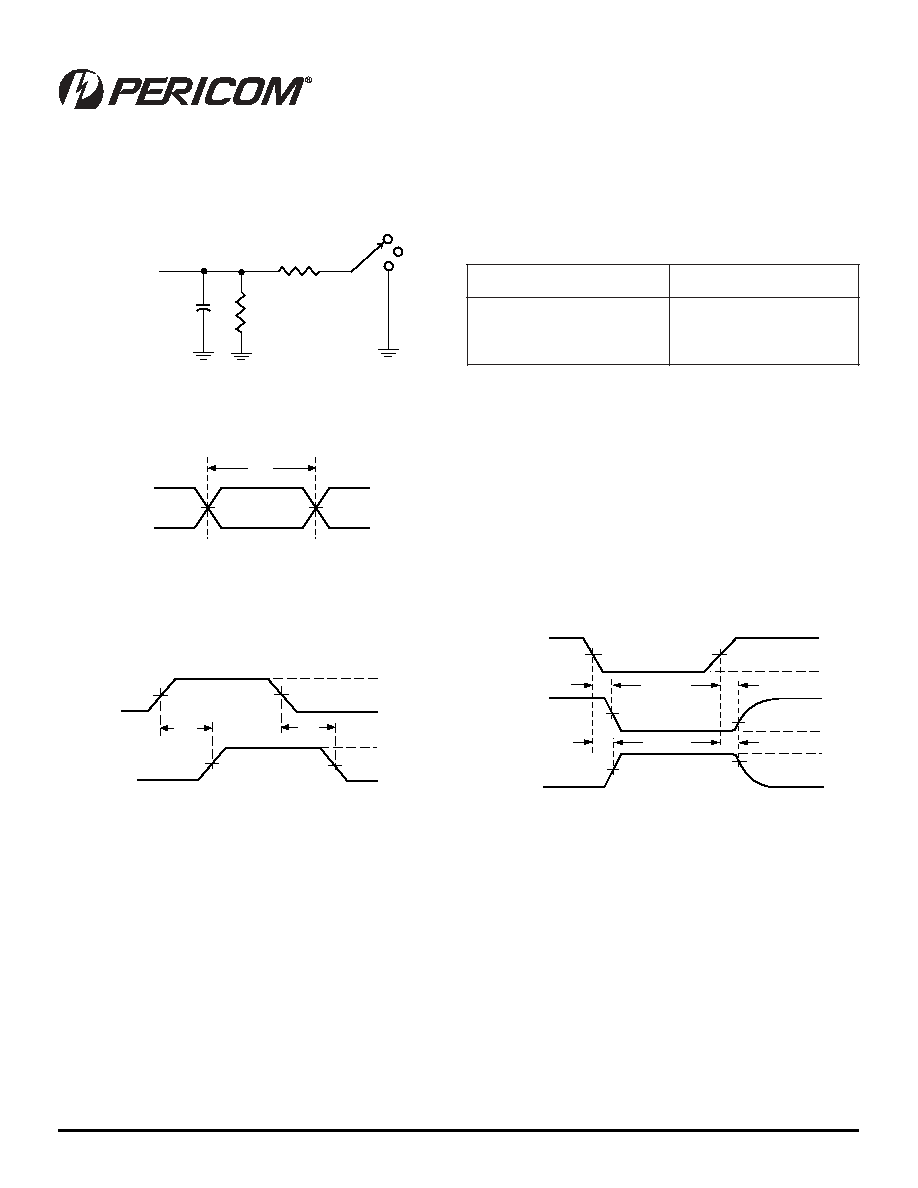
PARAMETER MEASUREMENT INFORMATION
V
CC
= 2.7V and 3.3V ±0.3V
Load Circuit
t
s
e
T
1
S
t
H
L
P
t/
L
H
P
t
Z
L
P
t/
L
Z
P
t
Z
H
P
t/
H
Z
P
n
e
p
O
V
6
D
N
G
Notes:
A. C
L
includes probe and jig capacitance.
B. Waveform 1 is for an output with internal conditions such that the output is low except when disabled by the output control.
Waveform 2 is for an output with internal conditions such that the output is high except when disabled by the output control.
C. All input impulses are supplied by generators having the following characteristics: PRR
10 MHz, Z
O
= 50
0
Ohm, t
R
2.5ns, t
F
2.5ns.
D. The outputs are measured one at a time with one transition per measurement.
Figure 1. Load Circuit and Voltage Waveforms
500
500
6V
Open
GND
S1
From Output
Under Test
CL = 50pF
(See Note A)
Voltage Waveforms
Propagation Delay Times
Voltage Waveforms
Enable and Disable Times
Voltage Waveforms
Pulse Duration
Input
t
PLH
t
PHL
0V
Output
V
OH
V
OL
1.5V
1.5V
1.5V
2.7V
1.5V
Input
t
W
1.5V
2.7V
1.5V
0V
tPZL
Output
Control
(Low Level
Enabling)
0V
1.5V
1.5V
1.5V
1.5V
tPLZ
tPHZ
VOL+0.3V
3V
0V
tPZH
Output
Waveform 1
S1 at 6V
(see Note B)
Output
Waveform 2
S1 at GND
(see Note B)
VOH -0.3V
VOH
VOL
2.7V
PI74LVTC244
3.3V 8-Bit Buffers/Line Drivers
with 3-State Outputs
7
PS8691 07/01/03
12345678901234567890123456789012123456789012345678901234567890121234567890123456789012345678901212345678901234567890123456789012123456789012
12345678901234567890123456789012123456789012345678901234567890121234567890123456789012345678901212345678901234567890123456789012123456789012
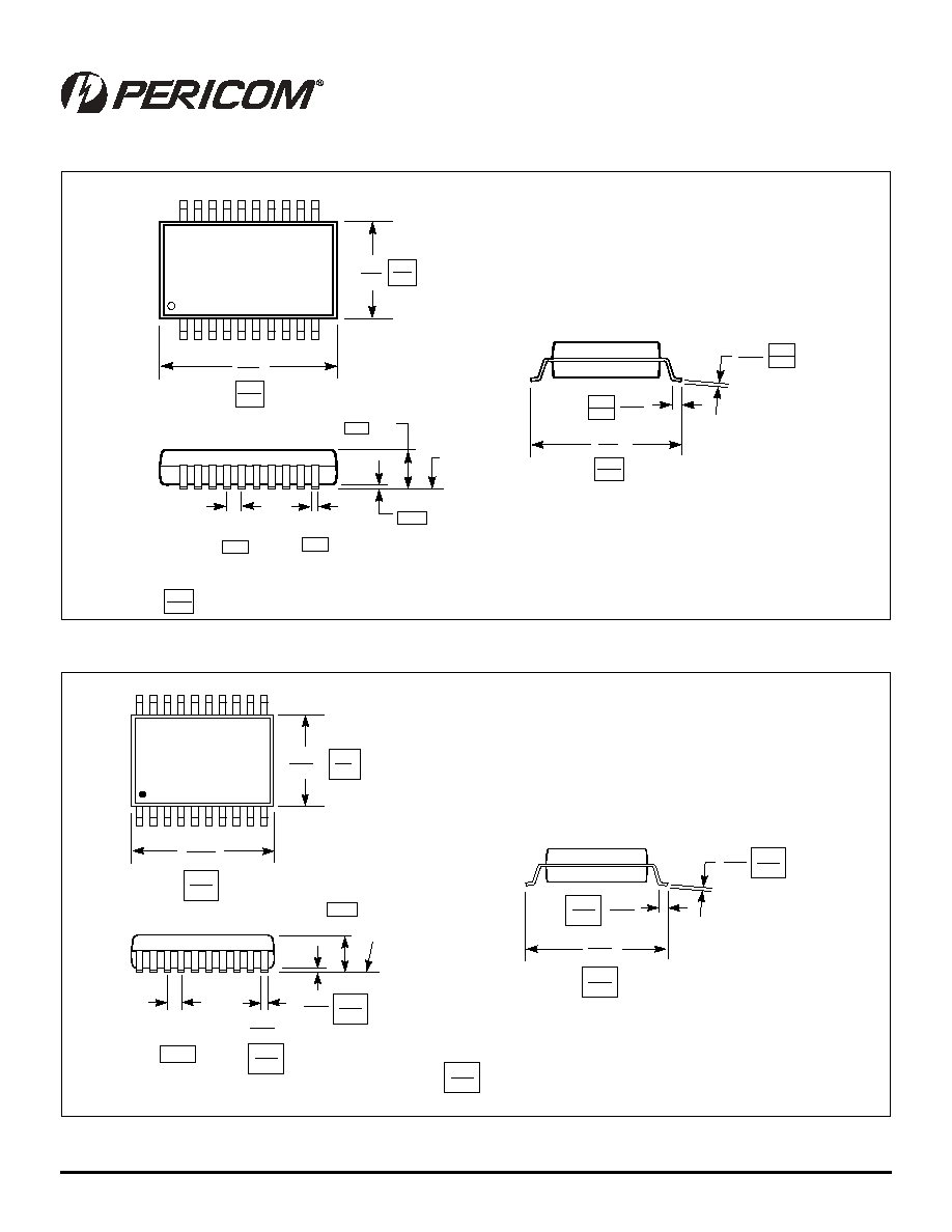
Packaging Mechanical: 20-pin SSOP (H)
Packaging Mechanical: 20-pin TSSOP (L)
.272
.295
.078
.002
SEATING
PLANE
.0098
Max.
.0256
BSC
.022
.037
.004
.009
.291
.322
1
20
.197
.220
0.25
X.XX
X.XX
DENOTES DIMENSIONS
IN MILLIMETERS
0.050
7.40
8.20
0.55
0.95
0.09
0.25
5.00
5.60
2.00
6.90
7.50
0.65
Max
Min
.252
.260
.047
1.20
.002
.006
SEATING
PLANE
.0256
BSC
.018
.030
.004
.008
.238
.269
1
20
.169
.177
X.XX
X.XX
DENOTES CONTROLLING
DIMENSIONS IN MILLIMETERS
0.05
0.15
6.1
6.7
0.45
0.75
0.09
0.20
4.3
4.5
6.4
6.6
0.65
0.19
0.30
.007
.012
Max
8
PS8691 07/01/03
PI74LVTC244
3.3V 8-Bit Buffers/Line Drivers
with 3-State Outputs
12345678901234567890123456789012123456789012345678901234567890121234567890123456789012345678901212345678901234567890123456789012123456789012
12345678901234567890123456789012123456789012345678901234567890121234567890123456789012345678901212345678901234567890123456789012123456789012
Pericom Semiconductor Corporation
2380 Bering Drive ∑ San Jose, CA 95131 ∑ 1-800-435-2336 ∑ Fax (408) 435-1100 ∑ http://www.pericom.com
e
d
o
C
g
n
i
r
e
d
r
O
e
d
o
C
g
n
i
g
a
k
c
a
P
n
o
i
t
p
i
r
c
s
e
D
H
4
4
2
C
T
V
L
4
7
I
P
H
P
O
S
S
c
it
s
a
l
p
e
d
i
w
li
m
-
9
0
2
,
n
i
p
-
0
2
L
4
4
2
C
T
V
L
4
7
I
P
L
P
O
S
S
T
c
it
s
a
l
p
e
d
i
w
li
m
-
3
7
1
,
n
i
p
-
0
2
S
4
4
2
C
T
V
L
4
7
I
P
S
C
I
O
S
c
it
s
a
l
p
e
d
i
w
li
m
-
0
0
3
,
n
i
p
-
0
2
Ordering Information
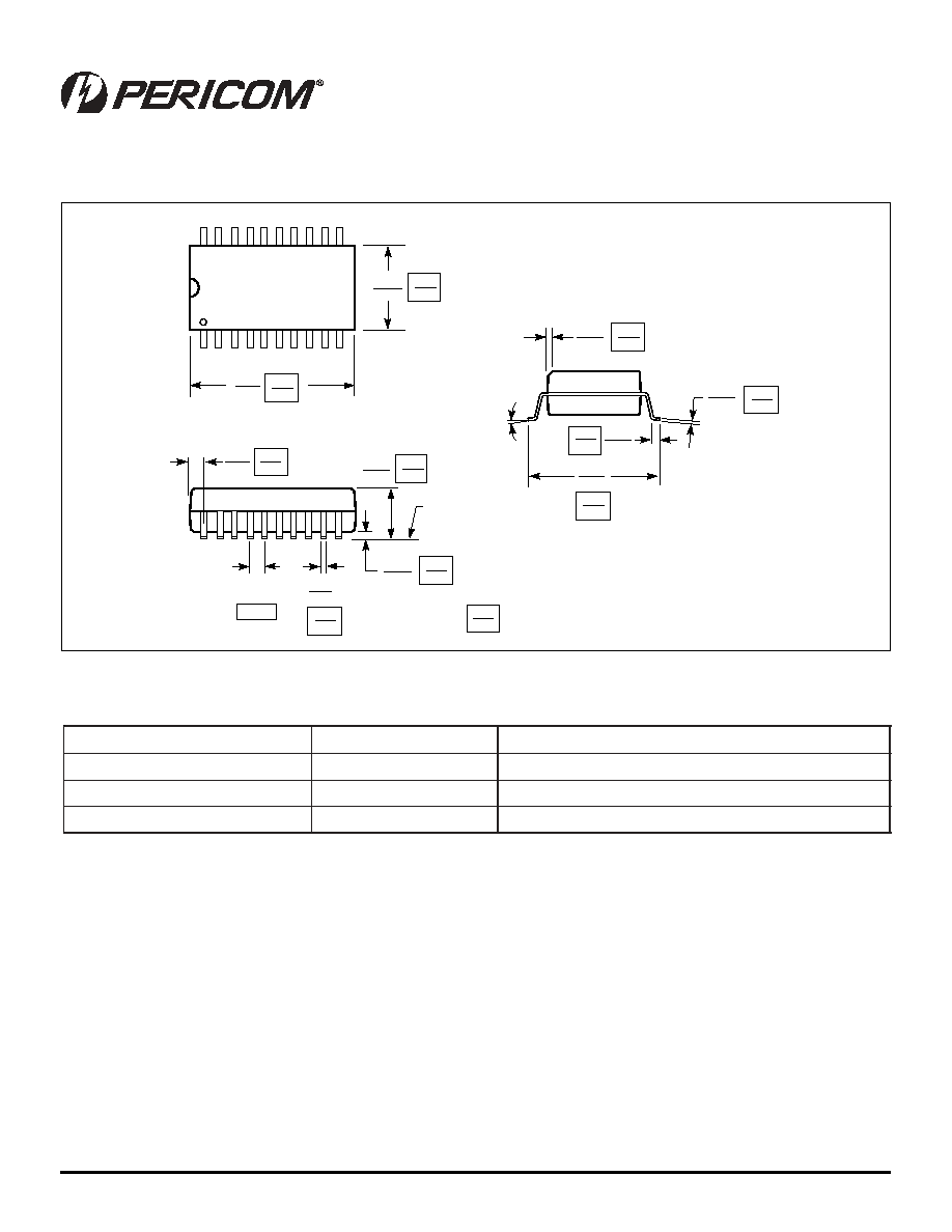
Packaging Mechanical: 20-pin SOIC (S)
SEATING
PLANE
.050
BSC
1
20
0-8∞
.2914
.2992
X.XX
X.XX
DENOTES CONTROLLING
DIMENSIONS IN MILLIMETERS
7.40
7.60
.496
.511
12.60
12.99
1.27
.0926
.1043
2.35
2.65
.394
.419
10.00
10.65
.0040
.0118
0.10
0.30
.013
.020
0.33
0.51
.010
.029
0.254
0.737
.0091
.0125
0.23
0.32
0.41
1.27
.016
.050
x 45∞
.020
.030
0.508
0.762
REF
Notes:
1. Thermal characteristics can be found on the company web site at http://www.pericom.com/packaging/mechanicals.php