
1
PS8565B 07/07/04
GND
V
CC
Y
OUT
A
IN
B
IN
1
2
4
5
3
12345678901234567890123456789012123456789012345678901234567890121234567890123456789012345678901212345678901234567890123456789012123456789012
12345678901234567890123456789012123456789012345678901234567890121234567890123456789012345678901212345678901234567890123456789012123456789012
SOTiny
TM
Gate STX
2-Input
Features
∑ High-speed: t
PD
= 2.4ns typical into 50pF @ 5V V
CC
∑ Broad operating range: V
CC
= 1.65V ≠ 5.5V
∑ Power down high-impedance inputs/outputs
∑ High output drive: ±24mA at 3V V
CC
∑ Packaging:
-5-pin SOT23 (T)
-5-pin SC70 (C)
Description
The PI74STX1G08 is a 2-Input AND Gate that operates over the
1.65V to 5.5V V
CC
operating range.
Pericom's PI74STX series of products are produced using the
Company's advanced submicron technology.
PI74STX1G08
Block Diagram
Pin Configuration
5-Pin
T, C
A
IN
BIN
YOUT
s
t
u
p
n
I
t
u
p
t
u
O
A
N
I
B
N
I
Y
T
U
O
L
L
H
H
L
H
L
H
L
L
L
H
Function Table
Note:
H = HIGH Logic Level
L = LOW Logic Level
Pin Description
s
e
m
a
N
n
i
P
n
o
i
t
p
i
r
c
s
e
D
A
N
I
t
u
p
n
I
B
N
I
t
u
p
n
I
Y
T
U
O
t
u
p
t
u
O
Recommended Operating Conditions
(1)
Note:
1. Unused inputs must be held HIGH or LOW. They may not float.
r
e
t
e
m
a
r
a
P
n
o
i
t
i
d
n
o
C
.
n
i
M
.
x
a
M
s
t
i
n
U
V
(
e
g
a
tl
o
V
y
l
p
p
u
S
C
C
)
5
6
.
1
5
.
5
V
V
(
e
g
a
tl
o
V
t
u
p
n
I
N
I
)
0
5
.
5
V
(
e
g
a
tl
o
V
t
u
p
t
u
O
T
U
O
)
0
V
C
C
e
r
u
t
a
r
e
p
m
e
T
g
n
it
a
r
e
p
O
0
4
≠
5
8
C
∞
d
n
a
e
s
i
R
t
u
p
n
I
t
(
e
m
i
T
ll
a
F
r
t,
f
)
V
C
C
,
V
8
.
1
=
V
2
.
0
±
V
5
.
2
0
0
2
V
/
s
n
V
C
C
,
V
3
.
3
=
V
3
.
0
±
0
0
1
V
C
C
,
V
0
.
5
=
V
5
.
0
±
0
5

2
PS8565B 07/07/04
12345678901234567890123456789012123456789012345678901234567890121234567890123456789012345678901212345678901234567890123456789012123456789012
12345678901234567890123456789012123456789012345678901234567890121234567890123456789012345678901212345678901234567890123456789012123456789012
PI74STX1G08
SOTiny
TM
Gate STX
2-Input AND
DC Electrical Characteristics
(Over supply voltage and operating temperature ranges, unless otherwise specified)
l
o
b
m
y
S
r
e
t
e
m
a
r
a
P
V
C
C
)
V
(
s
n
o
i
t
i
d
n
o
C
T
A
C
∞
5
2
+
=
T
A
C
∞
5
8
+
o
t
0
4
≠
=
s
t
i
n
U
.
n
i
M
.
p
y
T
.
x
a
M
.
n
i
M
.
x
a
M
V
H
I
l
e
v
e
L
H
G
I
H
e
g
a
tl
o
V
t
u
p
n
I
5
9
.
1
-
5
6
.
1
5
.
5
-
3
.
2
V
5
7
.
0
C
C
V
0
7
.
0
C
C
V
5
7
.
0
C
C
V
0
7
.
0
C
C
V
V
L
I
l
e
v
e
L
W
O
L
e
g
a
tl
o
V
t
u
p
n
I
5
9
.
1
-
5
6
.
1
5
.
5
-
3
.
2
V
5
2
.
0
C
C
V
0
3
.
0
C
C
V
5
2
.
0
C
C
V
0
3
.
0
C
C
V
H
O
l
e
v
e
L
H
G
I
H
e
g
a
tl
o
V
t
u
p
t
u
O
5
6
.
1
8
.
1
3
.
2
0
.
3
5
.
4
V
N
I
V
=
L
I
I
H
O
A
µ
0
0
1
≠
=
5
5
.
1
7
.
1
2
.
2
9
.
2
4
.
4
5
6
.
1
9
7
.
1
9
2
.
2
9
9
.
2
5
.
4
5
5
.
1
7
.
1
2
.
2
9
.
2
4
.
4
5
6
.
1
3
.
2
0
.
3
0
.
3
5
.
4
I
H
O
A
m
4
≠
=
I
H
O
A
m
8
≠
=
I
H
O
A
m
6
1
≠
=
I
H
O
A
m
4
2
≠
=
I
H
O
A
m
2
3
≠
=
9
2
.
1
9
.
1
4
.
2
3
.
2
8
.
3
2
5
.
1
3
1
.
2
1
7
.
2
5
5
.
2
0
2
.
4
9
2
.
1
9
.
1
4
.
2
3
.
2
8
.
3
V
L
O
l
e
v
e
L
W
O
L
e
g
a
tl
o
V
t
u
p
t
u
O
5
6
.
1
8
.
1
3
.
2
0
.
3
5
.
4
V
N
I
V
=
H
I
I
L
O
A
µ
0
0
1
=
1
0
.
0
1
0
.
0
1
0
.
0
0
0
.
0
0
0
.
0
1
.
0
1
.
0
1
.
0
1
.
0
1
.
0
1
.
0
1
.
0
1
.
0
1
.
0
1
.
0
5
6
.
1
3
.
2
0
.
3
0
.
3
5
.
4
I
L
O
A
m
4
=
I
L
O
A
m
8
=
I
L
O
A
m
6
1
=
I
L
O
A
m
4
2
=
I
L
O
A
m
2
3
=
8
0
.
0
0
1
.
0
8
1
.
0
8
2
.
0
8
2
.
0
4
2
.
0
3
.
0
4
.
0
5
5
.
0
5
5
.
0
4
2
.
0
3
.
0
4
.
0
5
5
.
0
5
5
.
0
I
N
I
e
g
a
k
a
e
L
t
u
p
n
I
t
n
e
r
r
u
C
5
.
5
-
0
V
N
I
D
N
G
,
V
5
.
5
=
1
≠
1
1
≠
1
A
µ
I
F
F
O
f
f
O
r
e
w
o
P
t
n
e
r
r
u
C
e
g
a
k
a
e
L
0
.
0
V
N
I
V
r
o
T
U
O
V
5
.
5
=
1
≠
1
1
≠
1
I
C
C
y
l
p
p
u
S
t
n
e
c
s
e
i
u
Q
t
n
e
r
r
u
C
5
.
5
-
5
6
.
1
V
N
I
D
N
G
,
V
5
.
5
=
0
.
2
0
2
Supply Voltage (V
CC
) .......................................... ≠0.5V to +6V
DC Input Voltage (V
IN
) ....................................... ≠0.5V to +6V
DC Output Voltage (V
OUT
) ................................. ≠0.5V to +6V
DC Input Diode Current (I
IK
) ........................ ≠50mA to 20mA
DC Output Diode Current (I
OK
) .................... ≠50mA to 20mA
DC Output Current (I
OUT
) ........................................... ±50mA
Absolute Maximum Ratings
Note:
Absolute maximum ratings are DC values beyond which the device may be damaged or have its useful life impaired. The datasheet specifications
should be met, without exception, to ensure that the system design is reliable over its power supply, temperature, and output/input loading
variables. Pericom does not recommend operation outside datasheet specifications.
DC V
CC
/GND Current (I
CC
/I
GND
) ................................ ±50mA
Storage Temperature (T
STG
) .......................... ≠65∞C to +150∞C
Junction Lead Temperature (IOS) ................................... 200∞C
Power Dissipation SOT23 ............................................ 200mW
SC70 ............................................... 150mW

3
PS8565B 07/07/04
12345678901234567890123456789012123456789012345678901234567890121234567890123456789012345678901212345678901234567890123456789012123456789012
12345678901234567890123456789012123456789012345678901234567890121234567890123456789012345678901212345678901234567890123456789012123456789012
PI74STX1G08
SOTiny
TM
Gate STX
2-Input AND
AC Loading and Waveforms
Figure 1. AC Test Circuit
Figure 2. I
CCD
Test Circuit
Figure 3. AC Waveforms
C
L
includes load and stray capacitance
Input PRR = 1.0 MHz; t
W
= 500ns
Input
R
L
C
L
V
CC
Output
Input = AC Waveform; t
r
= t
f
= 1.8ns;
PRR = 10 MHz; Duty Cycle = 50%
Input
V
CC
A
V
OH
GND
Input
Output
t
W
t
PLH
t
r
= 3ns
t
f
= 3ns
t
PHL
V
OL
50%
50%
50%
50%
90%
90%
10%
10%
V
CC
AC Electrical Characteristics
Notes:
3. C
PD
is defined as the value of the internal equivalent capacitance which is derived from dynamic operating current consumption (I
CCD
) at no
output loading and operating at 50% duty cycle (see Figure 2). C
PD
is related to I
CCD
dynamic operating current by the expression: I
CCD
=
(C
PD
)(V
CC
)(f
IN
) + (I
CC
static).
l
o
b
m
y
S
r
e
t
e
m
a
r
a
P
V
C
C
)
V
(
s
n
o
i
t
i
d
n
o
C
T
A
C
∞
5
2
+
=
T
A
C
∞
5
8
+
o
t
C
∞
0
4
≠
=
s
t
i
n
U
.
g
i
F
.
o
N
.
n
i
M
.
p
y
T
.
x
a
M
.
n
i
M
.
x
a
M
t
H
L
P
,
t
L
H
P
y
a
l
e
D
n
o
it
a
g
a
p
o
r
P
5
1
.
0
±
8
.
1
2
.
0
±
5
.
2
3
.
0
±
3
.
3
5
.
0
±
0
.
5
C
L
,
F
p
5
1
=
R
L
=
1
m
h
o
M
7
.
0
5
.
0
5
.
0
5
.
0
5
.
5
2
.
3
5
.
2
0
.
2
5
.
6
1
.
4
3
.
3
6
.
2
7
.
0
5
.
0
5
.
0
5
.
0
1
.
7
5
.
4
6
.
3
9
.
2
s
n
1
3
t
H
L
P
,
t
L
H
P
y
a
l
e
D
n
o
it
a
g
a
p
o
r
P
3
.
0
±
3
.
3
5
.
0
±
0
.
5
C
L
,
F
p
0
5
=
R
L
5
=
0
s
m
h
o
0
5
.
0
5
.
0
3
.
3
4
.
2
4
.
4
3
.
3
5
.
0
5
.
0
9
.
4
7
.
3
1
3
C
N
I
e
c
n
a
ti
c
a
p
a
C
t
u
p
n
I
0
4
F
p
C
D
P
n
o
it
a
p
i
s
s
i
D
r
e
w
o
P
e
c
n
a
ti
c
a
p
a
C
)
3
(
3
.
3
0
.
5
0
2
0
3
2
4
PS8565B 07/07/04
12345678901234567890123456789012123456789012345678901234567890121234567890123456789012345678901212345678901234567890123456789012123456789012
12345678901234567890123456789012123456789012345678901234567890121234567890123456789012345678901212345678901234567890123456789012123456789012
PI74STX1G08
SOTiny
TM
Gate STX
2-Input AND
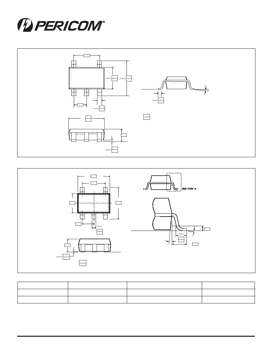
.102
.118
BSC
0.60
1
2
3
.000
.005
0.00
0.15
.014
.019
0.35
0.50
5
4
1.50
1.75
.059
.068
0.10
.023
.004
1.45 MAX.
SEATING
PLANE
.057
0" - 10"
1.90
.075
.037
BSC
2.60
3.00
0.95
.110
.118
2.80
3.00
X.XX
X.XX
Datum "A"
DENOTES DIMENSIONS
IN MILIMETERS
Packaging Mechanical: 5-Pin SOT23 (T)
GUAGE PLANE
SEATING PLANE
SEATING PLANE
DENOTES DIMENSIONS
IN MILLIMETERS
Notes:
1. Controlling dimensions in millimeters
2. Ref: JEDEC MO-203AA
BSC
VIEW A
BSC
REV
0
∞
-8
∞
4
∞
-10
∞
0.15
.321
0.42
.017
.010
.018
0.26
0.46
.006
3
4
5
2
1
.011
.026 0.65
BSC
.083
2.10
BSC
.049
1.25
BSC
.051
1.30
BSC
.079 2.00
0.15
0.30
MAX
.004
0.10
0
0
XXX
XXX
1.10
Packaging Mechanical: 5-Pin SC70 (C)
Pericom Semiconductor Corporation ∑ 1-800-435-2336 ∑ www.pericom.com
Ordering Information
Notes:
1. Thermal characteristics can be found on the company web site at www.pericom.com/packaging/
2. X = Tape and reel
Ordering Code
Package Code
Package Description
Top Marking
PI74STX1G08TX
T
5-pin, SOT23
B8
PI74STX1G08CX
C
5-pin, SC70
B8