DATASHEET SEARCH SITE | WWW.ALLDATASHEET.COM
1
PS8160C 09/27/04
Description
Pericom Semiconductor's PI74VCX16244 buffer/driver is designed
specifically to improve both the performance and density of 3-state
memory address drivers, clock drivers, and bus-oriented receivers
and transmitters.
The device can be used as four 4-bit buffers, two 8-bit buffers, or one
16-bit buffer. It provides true outputs and symmetrical active-low
output-enable (OE) inputs.
To ensure the high-impedance state during power up or power down,
OE should be tied to Vcc through a pullup resistor; the minimum
value of the resistor is determined by the current-sinking capability
of the driver.
The PI74VCX family is I/O Tolerant, allowing it to operate in
1.8/3.6V systems.
12345678901234567890123456789012123456789012345678901234567890121234567890123456789012345678901212345678901234567890123456789012123456789012
12345678901234567890123456789012123456789012345678901234567890121234567890123456789012345678901212345678901234567890123456789012123456789012
Features
· The PI74VCX Family is designed for low voltage
operation, C
D
= 1.8V to 3.6V
· 3.6V Tolerant Inputs and Outputs
· Supports Live Insertion
· Balanced Drive, ±24mA
· Uses patented Noise Reduction Circuitry
· Typical V
OLP
(Output Ground Bounce) <0.6V
at V
DD
= 2.5V, T
A
= 25ºC
· Typical V
OHV
(Output V
OH
Undershoot) < -0.6V
at V
DD
= 2.5V, T
A
= 25ºC
· Power-Off high impedance inputs and outputs
· Industrial operation at 40°C to +85°C
· Packaging (Pb-free & Green available):
48-pin 240-mil wide plastic TSSOP (A)
PI74VCX16244
16-Bit Buffer/Driver
with 3-State Outputs
Block Diagram
3
Y
1
3
Y
2
3
Y
3
3
Y
4
2
Y
1
2
Y
2
2
Y
3
2
Y
4
4
Y
1
4
Y
2
4
Y
3
4
Y
4
1
Y
2
1
Y
3
1
Y
4
1
Y
1
1
OE
1
A
1
1
A
2
1
A
3
1
A
4
3
OE
3
A
1
3
A
2
3
A
3
3
A
4
2
OE
2
A
1
2
A
2
2
A
3
2
A
4
4
OE
4
A
1
4
A
2
4
A
3
4
A
4
43
44
46
47
1
37
38
40
41
48
12
11
9
8
6
5
3
2
32
33
35
36
25
17
16
14
13
26
27
29
30
24
23
22
20
19
2
PS8160C 09/27/04
12345678901234567890123456789012123456789012345678901234567890121234567890123456789012345678901212345678901234567890123456789012123456789012
12345678901234567890123456789012123456789012345678901234567890121234567890123456789012345678901212345678901234567890123456789012123456789012
PI74VCX16244
16-Bit Buffer/Driver
with 3-State Outputs
1
2
3
4
5
6
7
8
9
48
10
47
11
46
12
45
13
44
14
43
15
42
16
41
17
40
18
39
19
38
20
37
21
36
22
35
23
34
24
33
32
31
30
29
28
27
26
25
Pin Name
Description
nOE
3-State Output Enable Inputs (Active LOW)
nAx
Inputs
nYx
3-State Outputs
GND
Ground
V
CC
Power
Pin Description
Truth Table
(1)
Notes:
1. H = High Signal Level
L = Low Signal Level
X = Don't Care or Irrelevant
Z = High Impedance
Pin Configuration
1
OE
1
Y
1
1
Y
2
GND
1
Y
3
1
Y
4
V
CC
2
Y
1
2
Y
2
GND
2
Y
3
2
Y
4
3
Y
1
3
Y
2
GND
3
Y
3
3
Y
4
V
CC
4
Y
1
4
Y
2
GND
4
Y
3
4
Y
4
4
OE
2
OE
1
A
1
1
A
2
GND
1
A
3
1
A
4
V
CC
2
A
1
2
A
2
GND
2
A
3
2
A
4
3
A
1
3
A
2
GND
3
A
3
3
A
4
V
CC
4
A
1
4
A
2
GND
4
A
3
4
A
4
3
OE
s
t
u
p
n
I
s
t
u
p
t
u
O
E
O
n
A
n
X
x
Y
n
L
H
H
L
L
L
H
X
Z
3
PS8160C 09/27/04
12345678901234567890123456789012123456789012345678901234567890121234567890123456789012345678901212345678901234567890123456789012123456789012
12345678901234567890123456789012123456789012345678901234567890121234567890123456789012345678901212345678901234567890123456789012123456789012
PI74VCX16244
16-Bit Buffer/Driver
with 3-State Outputs
Note:
Stresses greater than those listed under MAXIMUM
RATINGS may cause permanent damage to the device.
This is a stress rating only and functional operation of the
device at these or any other conditions above those indi-
cated in the operational sections of this specification is not
implied. Exposure to absolute maximum rating conditions
for extended periods may affect reliability.
Supply Voltage Range, V
DD
...........................................0.5V to 4.6V
Input Voltage Range, V
I
............................................... -0.5V to 4.6V
Output Voltage Range, V
O
(3-Stated) ........................... -0.5V to 4.6V
Output Voltage Range, V
O
(1)
(Active) ..................... -0.5V to V
CC
+0.5
DC Input Diode Current (I
IK
) V
I
<0V ...................................... -50mA
DC Output Diode Current (I
OK
)
V
O
<0V .................................................................................. -50mA
V
O
>V
DD
............................................................................... +50mA
DC Output Source/Sink Current (I
OH
/I
OL
) .............................. ±50mA
DC V
DD
or GND Current per Supply Pin (I
CC
or GND) ...... ±100mA
Storage Temperature Range, T
stg
.............................. 65
°
C to 150
°
C
Recommended Operating Conditions
(2)
Maximum Ratings
(Above which the useful life may be impaired. For user guidelines, not tested.)
Notes
1. Absolute maximum of I
O
must be observed.
2. Unused control inputs must be held HIGH or LOW to prevent them from floating.
3 As measured between 0.8V and 2.0V, V
DD
= 3.0V.
.
n
i
M
.
x
a
M
s
t
i
n
U
V
D
D
e
g
a
tl
o
v
y
l
p
p
u
S
g
n
it
a
r
e
p
O
8
.
1
6
.
3
V
y
l
n
O
n
o
it
n
e
t
e
R
a
t
a
D
2
.
1
6
.
3
V
H
I
e
g
a
tl
o
v
t
u
p
n
i
l
e
v
e
l
-
h
g
i
H
V
D
D
V
6
.
3
o
t
V
7
.
2
=
0
.
2
V
L
I
e
g
a
tl
o
v
t
u
p
n
i
l
e
v
e
l
-
w
o
L
V
D
D
V
6
.
3
o
t
V
7
.
2
=
8
.
0
V
I
e
g
a
tl
o
v
t
u
p
n
I
3
.
0
-
6
.
3
V
O
e
g
a
tl
o
v
t
u
p
t
u
O
e
t
a
t
S
e
v
it
c
A
0
V
D
D
e
t
a
t
S
f
f
O
0
6
.
3
I
O
I
n
i
t
n
e
r
r
u
c
t
u
p
t
u
O
H
O
I
/
L
O
V
D
D
V
6
.
3
o
t
V
0
.
3
=
V
D
D
V
7
.
2
o
t
V
3
.
2
=
V
D
D
V
8
.
1
=
4
2
±
8
1
±
6
±
A
m
/t
v
e
t
a
r
ll
a
f
r
o
e
s
i
r
n
o
it
s
i
s
n
a
r
t
t
u
p
n
I
)
3
(
0
0
1
V
/
s
n
T
A
e
r
u
t
a
r
e
p
m
e
t
ri
a
-
e
e
r
f
g
n
it
a
r
e
p
O
-
0
4
5
8
C
4
PS8160C 09/27/04
12345678901234567890123456789012123456789012345678901234567890121234567890123456789012345678901212345678901234567890123456789012123456789012
12345678901234567890123456789012123456789012345678901234567890121234567890123456789012345678901212345678901234567890123456789012123456789012
PI74VCX16244
16-Bit Buffer/Driver
with 3-State Outputs
Electrical Characteristics over Recommended Operating Free-Air Temperature Range
(unless otherwise noted)
DC Characteristics (2.7V<V
DD
3.6V)
r
e
t
e
m
a
r
a
P
s
n
o
i
t
i
d
n
o
C
V
D
D
.
n
i
M
.
p
y
T
.
x
a
M
s
t
i
n
U
V
H
I
e
g
a
tl
o
V
t
u
p
n
I
l
e
v
e
L
H
G
I
H
6
.
3
-
7
.
2
0
.
2
V
V
L
I
e
g
a
tl
o
V
t
u
p
n
I
l
e
v
e
L
W
O
L
8
.
0
V
H
O
e
g
a
tl
o
V
t
u
p
t
u
O
l
e
v
e
L
H
G
I
H
I
H
O
=
-
0
0
1
µ
A
V
D
D
2
.
0
-
I
H
O
=
-
A
m
2
1
7
.
2
2
.
2
I
H
O
=
-
A
m
8
1
0
.
3
4
.
2
I
H
O
=
-
A
m
4
2
2
.
2
V
L
O
e
g
a
tl
o
V
t
u
p
t
u
O
l
e
v
e
L
W
O
L
I
L
O
=
0
0
1
µ
A
6
.
3
-
7
.
2
2
.
0
I
L
O
= 2
1
A
m
7
.
2
4
.
0
I
L
O
= 8
1
A
m
0
.
3
4
.
0
I
L
O
= 4
2
A
m
5
5
.
0
I
I
t
n
e
r
r
u
C
e
g
a
k
a
e
L
t
u
p
n
I
V
I
=
,
V
0
.
0
V
I
=
V
6
.
3
6
.
3
0
.
5
±
µ
A
I
Z
O
e
g
a
k
a
e
L
t
u
p
t
u
O
E
T
A
T
S
-
3
0
V
O
V
6
.
3
V
I
V
=
H
I
V
r
o
L
I
6
.
3
-
7
.
2
0
1
±
I
F
F
O
t
n
e
r
r
u
C
e
g
a
k
a
e
L
F
F
O
-
r
e
w
o
P
0
V
(
I
V
,
O
)
V
6
.
3
0
0
1
I
D
D
t
n
e
r
r
u
C
y
l
p
p
u
S
t
n
e
c
s
e
i
u
Q
V
I
V
=
D
D
D
N
G
o
t
6
.
3
-
7
.
2
0
2
V
D
D
V
(
I
V
,
O
)
V
6
.
3
0
2
±
I
D
D
I
n
i
e
s
a
e
r
c
n
I
D
D
t
u
p
n
i
r
e
p
V
H
I
V
=
D
D
,
V
6
.
0
-
V
t
a
s
t
u
p
n
i
r
e
h
t
O
D
D
d
n
G
r
o
0
5
7
5
PS8160C 09/27/04
12345678901234567890123456789012123456789012345678901234567890121234567890123456789012345678901212345678901234567890123456789012123456789012
12345678901234567890123456789012123456789012345678901234567890121234567890123456789012345678901212345678901234567890123456789012123456789012
PI74VCX16244
16-Bit Buffer/Driver
with 3-State Outputs
s
r
e
t
e
m
a
r
a
P
s
n
o
i
t
i
d
n
o
C
V
D
D
.
n
i
M
.
p
y
T
.
x
a
M
s
t
i
n
U
V
H
I
e
g
a
tl
o
V
t
u
p
n
I
l
e
v
e
L
H
G
I
H
3
.
2
-
8
.
1
x
7
.
0
V
D
D
V
V
L
I
e
g
a
tl
o
V
t
u
p
n
I
l
e
v
e
L
W
O
L
V
x
2
.
0
D
D
V
H
O
e
g
a
tl
o
V
t
u
p
t
u
O
l
e
v
e
L
H
G
I
H
I
H
O
0
0
1
-
=
µ
A
8
.
1
V
D
D
2
.
0
-
I
H
O
A
m
6
-
=
4
.
1
V
L
O
e
g
a
tl
o
V
t
u
p
t
u
O
l
e
v
e
L
W
O
L
I
L
O
0
0
1
=
µ
A
2
.
0
I
L
O
A
m
6
=
3
.
0
I
I
t
n
e
r
r
u
C
e
g
a
k
a
e
L
t
u
p
n
I
V
I
V
8
.
1
=
I
V
,
V
0
.
0
=
0
.
5
±
µ
A
I
Z
O
e
g
a
k
a
e
L
t
u
p
t
u
O
E
T
A
T
S
-
3
0
V
O
V
6
.
3
V
I
V
=
H
I
V
r
o
L
I
0
1
±
I
F
F
O
t
n
e
r
r
u
C
e
g
a
k
a
e
L
F
F
O
-
r
e
w
o
P
0
V
(
I
V
,
O
)
V
6
.
3
0
0
1
I
D
D
t
n
e
r
r
u
C
y
l
p
p
u
S
t
n
e
c
s
e
i
u
Q
V
I
V
=
D
D
D
N
G
r
o
8
.
1
0
2
V
D
D
V
(
I
V
,
O
)
V
6
.
3
8
.
1
0
2
±
DC Characteristics (2.3V
V
DD
2.7V)
DC Characteristics (1.8V
V
DD
2.3V)
Electrical Characteristics over Recommended Operating Free-Air Temperature Range
(unless otherwise noted) (continued from previous page)
s
r
e
t
e
m
a
r
a
P
s
n
o
i
t
i
d
n
o
C
V
D
D
.
n
i
M
.
p
y
T
.
x
a
M
s
t
i
n
U
V
H
I
e
g
a
tl
o
V
t
u
p
n
I
l
e
v
e
L
H
G
I
H
7
.
2
-
3
.
2
6
.
1
V
V
L
I
e
g
a
tl
o
V
t
u
p
n
I
l
e
v
e
L
W
O
L
7
.
0
V
H
O
e
g
a
tl
o
V
t
u
p
t
u
O
l
e
v
e
L
H
G
I
H
I
H
O
0
0
1
-
=
µ
A
V
D
D
2
.
0
-
I
H
O
A
m
6
-
=
3
.
2
0
.
2
I
H
O
A
m
2
1
-
=
8
.
1
I
H
O
A
m
8
1
-
=
7
.
1
V
L
O
e
g
a
tl
o
V
t
u
p
t
u
O
l
e
v
e
L
W
O
L
I
L
O
0
0
1
=
µ
A
7
.
2
-
3
.
2
2
.
0
I
L
O
A
m
2
1
=
3
.
2
4
.
0
I
L
O
A
m
8
1
=
6
.
0
I
I
t
n
e
r
r
u
C
e
g
a
k
a
e
L
t
u
p
n
I
V
I
V
,
V
0
.
0
=
I
V
7
.
2
=
7
.
2
0
.
5
±
µ
A
I
Z
O
e
g
a
k
a
e
L
t
u
p
t
u
O
E
T
A
T
S
-
3
0
V
O
V
6
.
3
V
I
V
=
H
I
V
r
o
L
I
7
.
2
-
3
.
2
0
1
±
I
F
F
O
t
n
e
r
r
u
C
e
g
a
k
a
e
L
F
F
O
-
r
e
w
o
P
0
V
(
I
V
,
O
)
V
6
.
3
0
0
1
I
D
D
t
n
e
r
r
u
C
y
l
p
p
u
S
t
n
e
c
s
e
i
u
Q
V
I
V
=
D
D
D
N
G
r
o
7
.
2
-
3
.
2
0
2
V
D
D
V
(
I
V
,
O
)
V
6
.
3
0
2
±
6
PS8160C 09/27/04
12345678901234567890123456789012123456789012345678901234567890121234567890123456789012345678901212345678901234567890123456789012123456789012
12345678901234567890123456789012123456789012345678901234567890121234567890123456789012345678901212345678901234567890123456789012123456789012
PI74VCX16244
16-Bit Buffer/Driver
with 3-State Outputs
AC Electrical Characteristics
(1)
Notes
1. For CL = 50pF add approximatly 300ps to AC maximum specification
2. Skew is defined as the absolute value of the difference between the actual propagation delay for any
two separate outputs of the same device. The specification applies to any outputs switching in the
same direction, either HIGH or LOW (t
OSHL
)
or LOW to HIGH (t
OSLH
).
Capacitance
Dynamic Switching Characteristics
l
o
b
m
y
S
r
e
t
e
m
a
r
a
P
C
,
C
°
5
8
+
o
t
C
°
0
4
-
=
A
T
L
R
,
F
p
0
3
=
L
0
0
5
=
s
t
i
n
U
V
D
D
V
3
.
0
±
V
3
.
3
=
V
D
D
V
2
.
0
±
V
5
.
2
=
V
D
D
V
8
.
1
=
.
n
i
M
.
x
a
M
.
n
i
M
.
x
a
M
.
n
i
M
.
x
a
M
t
L
H
P
t
,
H
L
P
y
a
l
e
D
p
o
r
P
8
.
0
5
.
2
0
.
1
0
.
3
5
.
1
0
.
5
s
n
t
L
Z
P
t
,
H
Z
P
e
m
i
T
e
l
b
a
n
E
t
u
p
t
u
O
8
.
0
5
.
3
0
.
1
1
.
4
5
.
1
5
.
6
t
Z
L
P
t
,
Z
H
P
e
m
i
T
e
l
b
a
s
i
D
t
u
p
t
u
O
8
.
0
5
.
3
0
.
1
8
.
3
5
.
1
0
.
5
t
L
H
S
O
t
H
L
S
O
w
e
k
S
t
u
p
t
u
O
o
t
t
u
p
t
u
O
)
2
(
5
.
0
5
.
0
5
.
0
l
o
b
m
y
S
r
e
t
e
m
a
r
a
P
s
n
o
i
t
i
d
n
o
C
V
D
D
T
A
C
°
5
2
+
=
l
a
c
i
p
y
T
s
t
i
n
U
V
P
L
O
V
k
a
e
P
c
i
m
a
n
y
D
t
u
p
t
u
O
t
e
i
u
Q
L
O
C
L
V
,
F
p
0
5
=
H
I
V
=
D
D
V
,
L
I
V
0
=
8
.
1
5
.
2
3
.
3
5
2
.
0
6
.
0
8
.
0
V
V
V
L
O
V
y
e
ll
a
V
c
i
m
a
n
y
D
t
u
p
t
u
O
t
e
i
u
Q
L
O
C
L
V
,
F
p
0
5
=
H
I
V
=
D
D
V
,
L
I
V
0
=
8
.
1
5
.
2
3
.
3
5
2
.
0
-
6
.
0
-
8
.
0
-
V
V
H
O
V
y
e
ll
a
V
c
i
m
a
n
y
D
t
u
p
t
u
O
t
e
i
u
Q
H
O
C
L
V
,
F
p
0
5
=
H
I
V
=
D
D
V
,
L
I
V
0
=
8
.
1
5
.
2
3
.
3
5
.
1
9
.
1
2
.
2
l
o
b
m
y
S
r
e
t
e
m
a
r
a
P
s
n
o
i
t
i
d
n
o
C
C
º
5
2
+
=
A
T
l
a
c
i
p
y
T
s
t
i
n
U
C
N
I
e
c
n
a
ti
c
a
p
a
C
t
u
p
n
I
V
D
D
,
V
3
.
3
r
o
V
5
.
2
,
V
8
.
1
=
V
1
V
r
o
V
0
=
D
D
6
F
p
C
T
U
O
e
c
n
a
ti
c
a
p
a
C
t
u
p
t
u
O
V
1
V
r
o
V
0
=
,
D
D
V
D
D
V
3
.
3
r
o
V
5
.
2
,
V
8
.
1
=
7
C
D
P
e
c
n
a
ti
c
a
p
a
C
n
o
it
a
p
i
s
s
i
D
r
e
w
o
P
V
1
V
r
o
V
0
=
,
D
D
z
H
M
0
1
=
F
V
D
D
V
3
.
3
r
o
V
5
.
2
,
V
8
.
1
=
0
2
7
PS8160C 09/27/04
12345678901234567890123456789012123456789012345678901234567890121234567890123456789012345678901212345678901234567890123456789012123456789012
12345678901234567890123456789012123456789012345678901234567890121234567890123456789012345678901212345678901234567890123456789012123456789012
PI74VCX16244
16-Bit Buffer/Driver
with 3-State Outputs
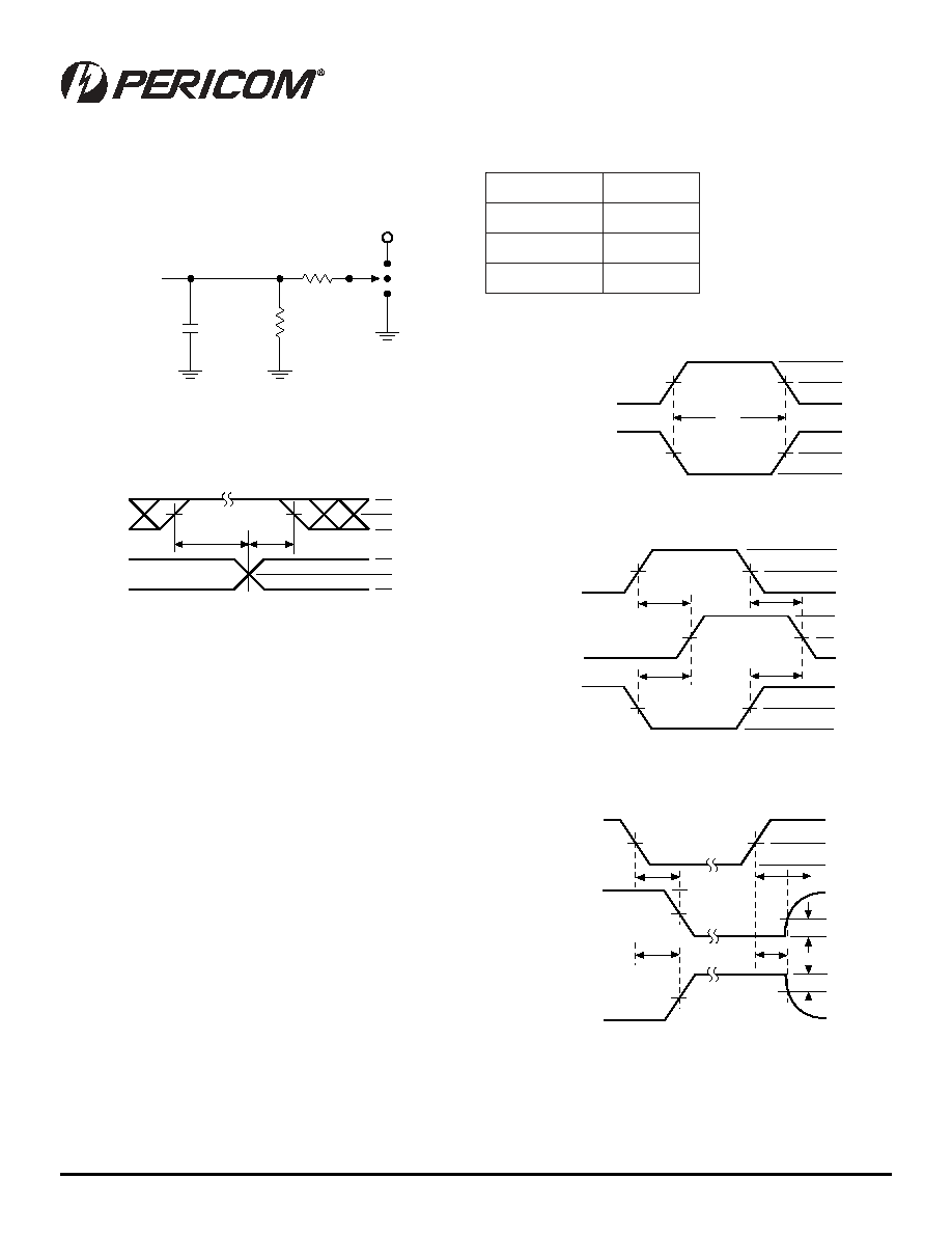
Test Circuits and Switching Waveforms
Parameter Measurement Information (V
DD
= 1.8V - 3.6V)
Setup, Hold, and Release Timing
Pulse Width
Switch Position
Propagaton Delay
Enable Disable Timing
Notes:
A. C
L
includes probe and jig capacitance.
B. Waveform 1 is for an output with internal conditions
such that the output is LOW except when disabled by
the output control.
Waveform 2 is for an output with internal conditions
such that the output is HIGH except when disabled by
the output control.
C. All input pulses are supplied by generators having the
following characteristics: PRR
10 MHz, Z
O
= 50
,
t
r
2ns, t
f
2ns, measured from 10% to 90%, unless
otherwise specified.
D. The outputs are measured one at a time with one
transition per measurement.
Output
Control
(Active LOW)
Output
Waveform 2
S1 at GND
(see Note B)
t
PZL
t
PLZ
V
DD
0V
V
DD
V
OL
0V
Output
Waveform 1
S1 at 2xV
DD
(see Note B)
+0.15V
-0.15V
V
OH
V
DD
t
PHZ
t
PZH
V
DD/2
V
DD/2
V
DD
/2
C
L
R
1
500
50pF
From Output
Under Test
GND
2 x V
DD
Open
(See Note A)
R
L
500
3
Low-High-Low
Pulse
t
W
High-Low-High
Pulse
V
DD
0V
V
DD
0V
V
DD/2
V
DD/2
Input
Opposite Phase
Input Transition
t
PLH
t
PHL
t
PLH
t
PHL
V
DD
0V
V
DD
V
OL
V
DD
0V
Output
V
DD/2
V
DD/2
V
DD/2
Data
Input
t
H
V
DD
t
SU
0V
Timing
Input
V
DD
0V
V
DD/2
V
DD/2
t
s
e
T
1
S
t d
p
n
e
p
O
t
Z
L
P
/t
L
Z
P
x
2 V
D
D
t
Z
H
P
/t
H
Z
P
D
N
G
8
PS8160C 09/27/04
12345678901234567890123456789012123456789012345678901234567890121234567890123456789012345678901212345678901234567890123456789012123456789012
12345678901234567890123456789012123456789012345678901234567890121234567890123456789012345678901212345678901234567890123456789012123456789012
PI74VCX16244
16-Bit Buffer/Driver
with 3-State Outputs
.236
.244
.488
.496
.002
.006
SEATING PLANE
.007
.010
.0197
BSC
.004
.008
.319
1
48
12.4
12.6
6.0
6.2
0.50
0.17
0.27
8.1
0.05
0.15
0.09
0.20
X.XX
X.XX
DENOTES DIMENSIONS
IN MILLIMETERS
.018
.030
0.45
0.75
.047
1.20 Max
BSC
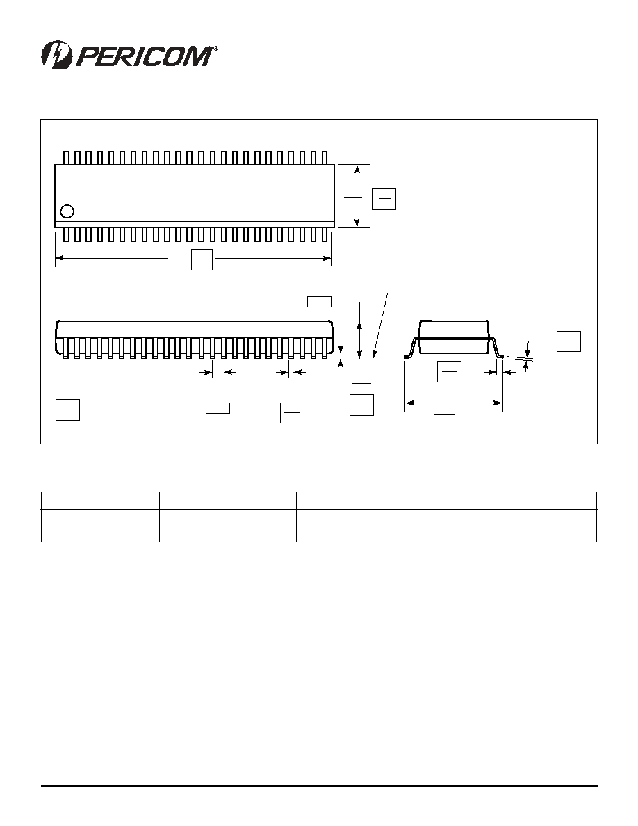
Packaging Mechanical: 48-pin TSSOP (A)
Ordering Information
Ordering Code
Package Code
Package Description
PI74VCX16244A
A
48-pin TSSOP
PI74VCX16244AE
A
Pb-free & Green, 48-pin TSSOP
Notes:
1. Thermal characteristics can be found on the company web site at www.pericom.com/packaging/
Pericom Semiconductor Corporation · 1-800-435-2336 · www.pericom.com