 | –≠–ª–µ–∫—Ç—Ä–æ–Ω–Ω—ã–π –∫–æ–º–ø–æ–Ω–µ–Ω—Ç: 1PS89SB16 | –°–∫–∞—á–∞—Ç—å:  PDF PDF  ZIP ZIP |

DATA SHEET
Product specification
Supersedes data of 1997 Jun 02
1999 Apr 27
DISCRETE SEMICONDUCTORS
PMBT2369
NPN switching transistor
book, halfpage
M3D088
1999 Apr 27
2
Philips Semiconductors
Product specification
NPN switching transistor
PMBT2369
FEATURES
∑
Low current (max. 200 mA)
∑
Low voltage (max. 15 V).
APPLICATIONS
∑
High-speed switching, especially in portable equipment.
DESCRIPTION
NPN switching transistor in a SOT23 plastic package.
MARKING
Note
1.
= p : Made in Hong Kong.
= t : Made in Malaysia.
TYPE NUMBER
MARKING CODE
(1)
PMBT2369
1J
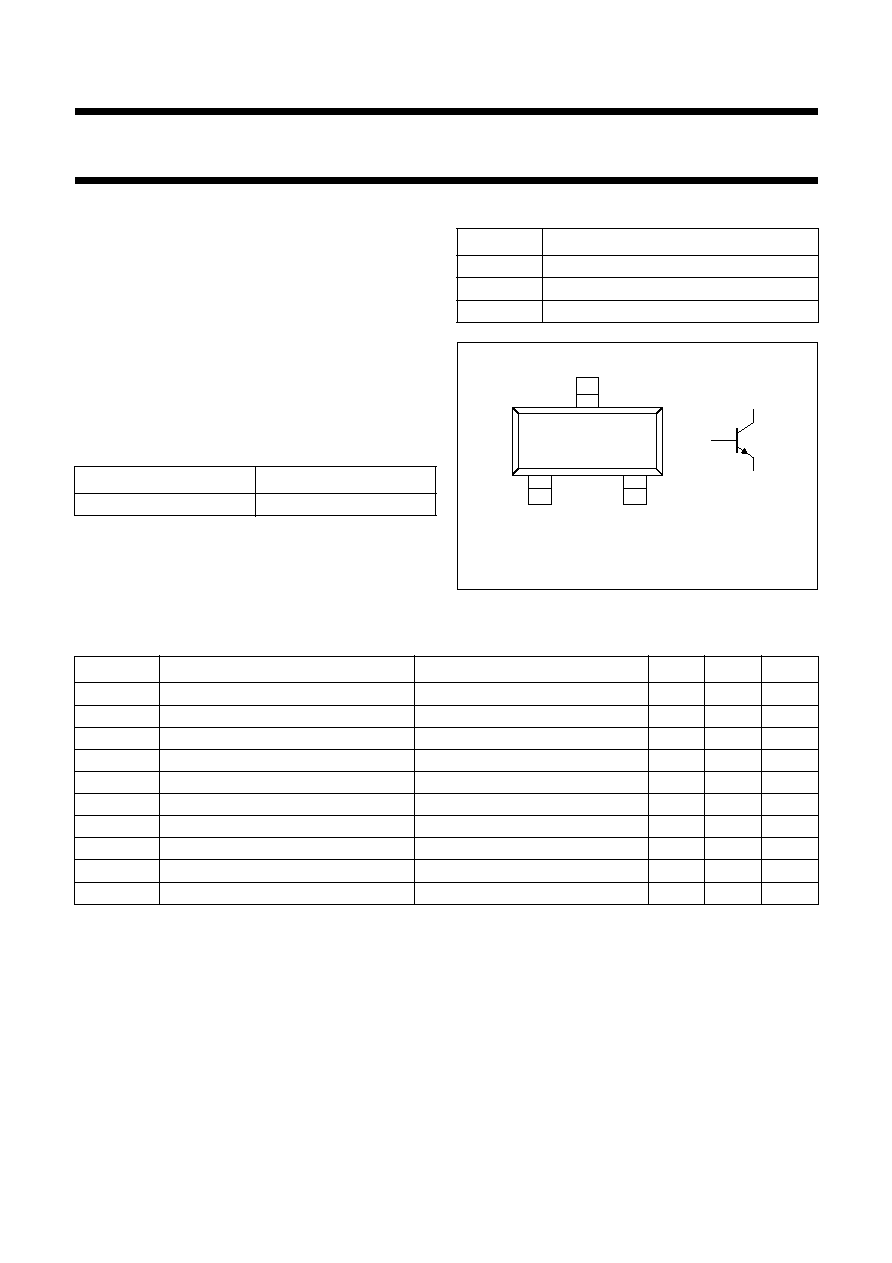
PINNING
PIN
DESCRIPTION
1
base
2
emitter
3
collector
Fig.1 Simplified outline (SOT23) and symbol.
handbook, halfpage
2
1
3
MAM255
Top view
2
3
1
LIMITING VALUES
In accordance with the Absolute Maximum Rating System (IEC 134).
Note
1. Transistor mounted on an FR4 printed-circuit board.
SYMBOL
PARAMETER
CONDITIONS
MIN.
MAX.
UNIT
V
CBO
collector-base voltage
open emitter
-
40
V
V
CEO
collector-emitter voltage
open base
-
15
V
V
EBO
emitter-base voltage
open collector
-
5
V
I
C
collector current (DC)
-
200
mA
I
CM
peak collector current
-
300
mA
I
BM
peak base current
-
100
mA
P
tot
total power dissipation
T
amb
25
∞
C; note 1
-
250
mW
T
stg
storage temperature
-
65
+150
∞
C
T
j
junction temperature
-
150
∞
C
T
amb
operating ambient temperature
-
65
+150
∞
C

1999 Apr 27
3
Philips Semiconductors
Product specification
NPN switching transistor
PMBT2369
THERMAL CHARACTERISTICS
Note
1. Transistor mounted on an FR4 printed-circuit board.
CHARACTERISTICS
T
j
= 25
∞
C unless otherwise specified.
SYMBOL
PARAMETER
CONDITIONS
VALUE
UNIT
R
th j-a
thermal resistance from junction to ambient
note 1
500
K/W
SYMBOL
PARAMETER
CONDITIONS
MIN.
MAX.
UNIT
I
CBO
collector cut-off current
I
E
= 0; V
CB
= 20 V
-
400
nA
I
E
= 0; V
CB
= 20 V; T
j
= 125
∞
C
-
30
µ
A
I
EBO
emitter cut-off current
I
C
= 0; V
EB
= 4 V
-
100
nA
h
FE
DC current gain
I
C
= 10 mA; V
CE
= 1 V
40
120
I
C
= 10 mA; V
CE
= 1 V; T
amb
=
-
55
∞
C
20
-
I
C
= 100 mA; V
CE
= 2 V
20
-
V
CEsat
collector-emitter saturation voltage
I
C
= 10 mA; I
B
= 1 mA
-
250
mV
V
BEsat
base-emitter saturation voltage
I
C
= 10 mA; I
B
= 1 mA
700
850
mV
C
c
collector capacitance
I
E
= i
e
= 0; V
CB
= 5 V; f = 1 MHz
-
4
pF
f
T
transition frequency
I
C
= 10 mA; V
CE
= 10 V; f = 100 MHz
500
-
MHz
Switching times (between 10% and 90% levels); (see Fig.2)
t
on
turn-on time
I
Con
= 10 mA; I
Bon
= 3 mA;
I
Boff
=
-
1.5 mA
-
10
ns
t
d
delay time
-
4
ns
t
r
rise time
-
6
ns
t
off
turn-off time
-
20
ns
t
s
storage time
-
10
ns
t
f
fall time
-
10
ns
1999 Apr 27
4
Philips Semiconductors
Product specification
NPN switching transistor
PMBT2369
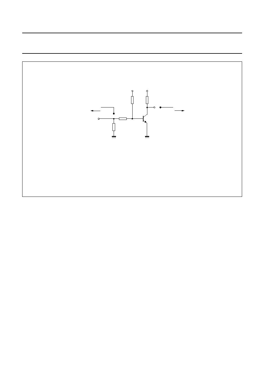
V
i
= 0.5 to 4.2 V; T = 500
µ
s; t
p
= 10
µ
s; t
r
= t
f
3 ns.
R1 = 56
; R2 = 1 k
; R
B
= 1 k
; R
C
= 270
.
V
BB
= 0.2 V; V
CC
= 2.7 V.
Oscilloscope input impedance Z
i
= 50
.
handbook, full pagewidth
RC
R2
R1
DUT
MLB826
Vo
RB
(probe)
450
(probe)
450
oscilloscope
oscilloscope
VBB
Vi
VCC
Fig.2 Test circuit for switching times.
1999 Apr 27
5
Philips Semiconductors
Product specification
NPN switching transistor
PMBT2369
PACKAGE OUTLINE
UNIT
A
1
max.
b
p
c
D
E
e
1
H
E
L
p
Q
w
v
REFERENCES
OUTLINE
VERSION
EUROPEAN
PROJECTION
ISSUE DATE
97-02-28
IEC
JEDEC
EIAJ
mm
0.1
0.48
0.38
0.15
0.09
3.0
2.8
1.4
1.2
0.95
e
1.9
2.5
2.1
0.55
0.45
0.1
0.2
DIMENSIONS (mm are the original dimensions)
0.45
0.15
SOT23
bp
D
e1
e
A
A1
Lp
Q
detail X
HE
E
w
M
v
M
A
B
A
B
0
1
2 mm
scale
A
1.1
0.9
c
X
1
2
3
Plastic surface mounted package; 3 leads
SOT23