1999 Sep 29
2
Philips Semiconductors
Product specification
Quad buffer/line driver; 3-state
74AHC126; 74AHCT126
FEATURES
∑
ESD protection:
HBM EIA/JESD22-A114-A
exceeds 2000 V
MM EIA/JESD22-A115-A
exceeds 200 V
CDM EIA/JESD22-C101
exceeds 1000 V
∑
Balanced propagation delays
∑
All inputs have Schmitt-trigger
actions
∑
Inputs accepts voltages higher than
V
CC
∑
For AHC only:
operates with CMOS input levels
∑
For AHCT only:
operates with TTL input levels
∑
Specified from
-
40 to +85 and +125
∞
C.
DESCRIPTION
The 74AHC/AHCT126 are
high-speed Si-gate CMOS devices
and are pin compatible with low
power Schottky TTL (LSTTL). They
are specified in compliance with
JEDEC standard No. 7A.
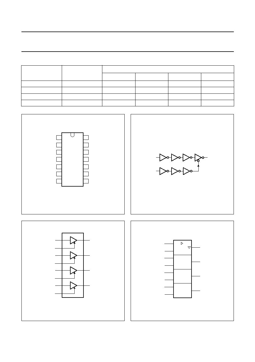
The 74AHC/AHCT126 are four
non-inverting buffer/line drivers with
3-state outputs. The 3-state outputs
(nY) are controlled by the output
enable input (nOE) A LOW at nOE
causes the outputs to assume a
HIGH-impedance OFF state.
The `126' is identical to the `125' but
has active HIGH enable inputs.
FUNCTION TABLE
See note 1.
Note
1. H = HIGH voltage level;
L = LOW voltage level;
X = don't care;
Z = high-impedance OFF state.
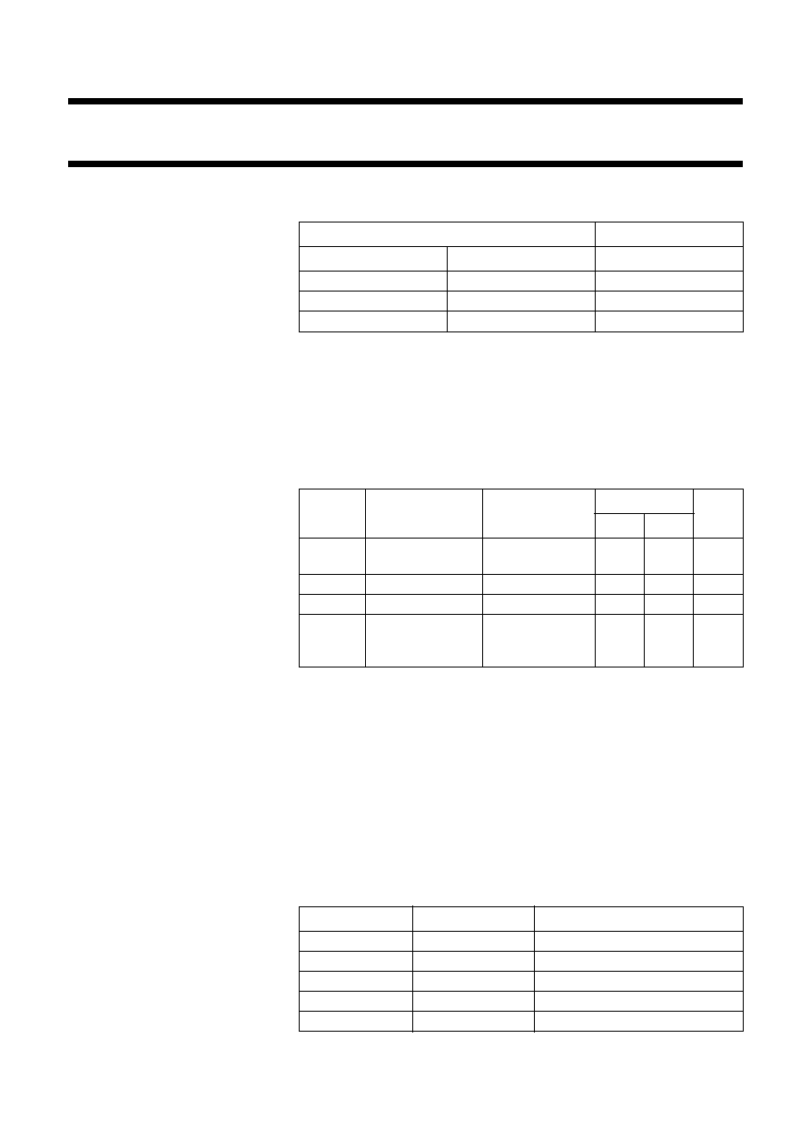
QUICK REFERENCE DATA
GND = 0 V; T
amb
= 25
∞
C; t
r
= t
f
3.0 ns.
Notes
1. C
PD
is used to determine the dynamic power dissipation (P
D
in
µ
W).
P
D
= C
PD
◊
V
CC
2
◊
f
i
+
(C
L
◊
V
CC
2
◊
f
o
) where:
f
i
= input frequency in MHz;
f
o
= output frequency in MHz;
(C
L
◊
V
CC
2
◊
f
o
) = sum of outputs;
C
L
= output load capacitance in pF;
V
CC
= supply voltage in Volts.
2. The condition is V
I
= GND to V
CC
.
PINNING
INPUTS
OUTPUT
nOE
nA
nY
H
L
L
H
H
H
L
X
Z
SYMBOL
PARAMETER
CONDITIONS
TYPICAL
UNIT
AHC
AHCT
t
PHL
/t
PLH
propagation delay
nA to nY
C
L
= 15 pF;
V
CC
= 5 V
3.3
3.0
ns
C
I
input capacitance
V
I
= V
CC
or GND
3.0
3.0
pF
C
O
output capacitance
4.0
4.0
pF
C
PD
power dissipation
capacitance
C
L
= 50 pF;
f = 1 MHz;
notes 1 and 2
10
12
pF
PIN
SYMBOL
DESCRIPTION
1, 4, 10 and 13
1OE to 4OE
output enable inputs (active HIGH)
2, 5, 9 and 12
1A to 4A
data inputs
3, 6, 8 and 11
1Y to 4Y
data outputs
7
GND
ground (0 V)
14
V
CC
DC supply voltage

1999 Sep 29
4
Philips Semiconductors
Product specification
Quad buffer/line driver; 3-state
74AHC126; 74AHCT126
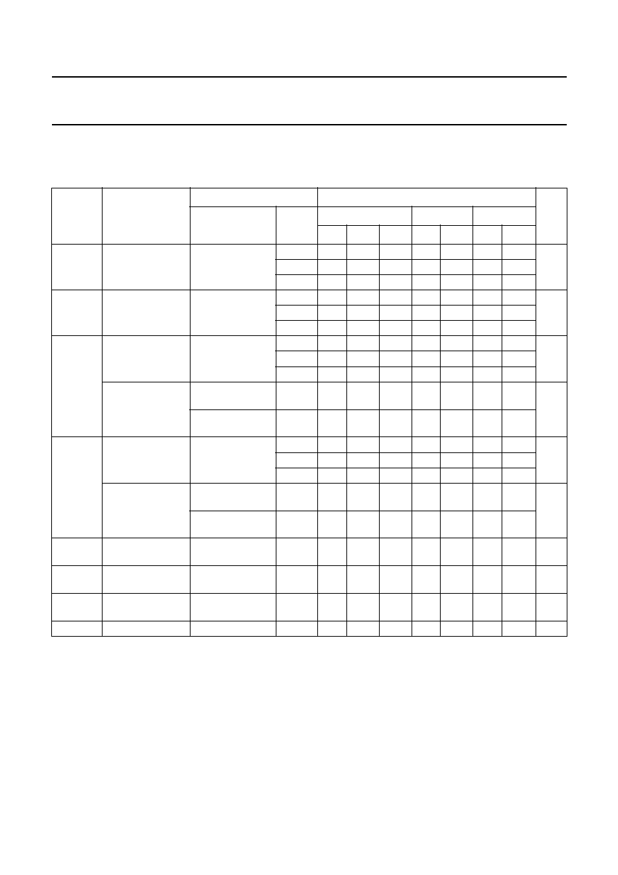
RECOMMENDED OPERATING CONDITIONS
LIMITING VALUES
In accordance with the Absolute Maximum Rating System (IEC 134); voltages are referenced to GND (ground = 0 V).
Notes
1. The input and output voltage ratings may be exceeded if the input and output current ratings are observed.
2. For SO packages: above 70
∞
C the value of P
D
derates linearly with 8 mW/K.
For TSSOP packages: above 60
∞
C the value of P
D
derates linearly with 5.5 mW/K.
SYMBOL
PARAMETER
CONDITIONS
74AHC
74AHCT
UNIT
MIN.
TYP.
MAX.
MIN.
TYP.
MAX.
V
CC
DC supply voltage
2.0
5.0
5.5
4.5
5.0
5.5
V
V
I
input voltage
0
-
5.5
0
-
5.5
V
V
O
output voltage
0
-
V
CC
0
-
V
CC
V
T
amb
operating ambient temperature
range
see DC and AC
characteristics per
device
-
40
+25
+85
-
40
+25
+85
∞
C
-
40
+25
+125
-
40
+25
+125
∞
C
t
r
,t
f
(
t/
f) input rise and fall rates
V
CC
= 3.3 V
±
0.3 V
-
-
100
-
-
-
ns/V
V
CC
= 5 V
±
0.5 V
-
-
20
-
-
20
SYMBOL
PARAMETER
CONDITIONS
MIN.
MAX. UNIT
V
CC
DC supply voltage
-
0.5
+7.0
V
V
I
input voltage range
-
0.5
+7.0
V
I
IK
DC input diode current
V
I
<
-
0.5 V; note 1
-
-
20
mA
I
OK
DC output diode current
V
O
<
-
0.5 V or V
O
> V
CC
+ 0.5 V; note 1
-
±
20
mA
I
O
DC output source or sink current
-
0.5 V < V
O
< V
CC
+ 0.5 V
-
±
25
mA
I
CC
DC V
CC
or GND current
-
±
75
mA
T
stg
storage temperature range
-
65
+150
∞
C
P
D
power dissipation per package
for temperature range:
-
40 to +125
∞
C; note 2
-
500
mW
1999 Sep 29
5
Philips Semiconductors
Product specification
Quad buffer/line driver; 3-state
74AHC126; 74AHCT126
DC CHARACTERISTICS
74AHC family
Over recommended operating conditions; voltages are referenced to GND (ground = 0 V).
SYMBOL
PARAMETER
TEST CONDITIONS
T
amb
(
∞
C)
UNIT
OTHER
V
CC
(V)
25
-
40 to +85
-
40 to +125
MIN.
TYP.
MAX. MIN. MAX. MIN. MAX.
V
IH
HIGH-level input
voltage
2.0
1.5
-
-
1.5
-
1.5
-
V
3.0
2.1
-
-
2.1
-
2.1
-
5.5
3.85
-
-
3.85
-
3.85
-
V
IL
LOW-level input
voltage
2.0
-
-
0.5
-
0.5
-
0.5
V
3.0
-
-
0.9
-
0.9
-
0.9
5.5
-
-
1.65
-
1.65
-
1.65
V
OH
HIGH-level output
voltage; all
outputs
V
I
= V
IH
or V
IL
;
I
O
=
-
50
µ
A
2.0
1.9
2.0
-
1.9
-
1.9
-
V
3.0
2.9
3.0
-
2.9
-
2.9
-
4.5
4.4
4.5
-
4.4
-
4.4
-
HIGH-level output
voltage
V
I
= V
IH
or V
IL
;
I
O
=
-
4.0 mA
3.0
2.58
-
-
2.48
-
2.40
-
V
V
I
= V
IH
or V
IL
;
I
O
=
-
8.0 mA
4.5
3.94
-
-
3.8
-
3.70
-
V
OL
LOW-level output
voltage; all
outputs
V
I
= V
IH
or V
IL
;
I
O
= 50
µ
A
2.0
-
0
0.1
-
0.1
-
0.1
V
3.0
-
0
0.1
-
0.1
-
0.1
4.5
-
0
0.1
-
0.1
-
0.1
LOW-level output
voltage
V
I
= V
IH
or V
IL
;
I
O
= 4 mA
3.0
-
-
0.36
-
0.44
-
0.55
V
V
I
= V
IH
or V
IL
;
I
O
= 8 mA
4.5
-
-
0.36
-
0.44
-
0.55
I
I
input leakage
current
V
I
= V
CC
or GND
5.5
-
-
0.1
-
1.0
-
2.0
µ
A
I
OZ
3-state output
OFF current
V
I
= V
IH
or V
IL
;
V
O
= V
CC
or GND
5.5
-
-
±
0.25
-
±
2.5
-
±
10.0
µ
A
I
CC
quiescent supply
current
V
I
= V
CC
or GND;
I
O
= 0
5.5
-
-
2.0
-
20
-
40
µ
A
C
I
input capacitance
-
-
3
10
-
10
-
10
pF