1999 Sep 01
2
Philips Semiconductors
Product specification
Dual 2-to-4 line decoder/demultiplexer
74AHC139;
74AHCT139
FEATURES
∑
ESD protection:
HBM EIA/JESD22-A114-A exceeds 2000 V
MM EIA/JESD22-A115-A exceeds 200 V
CDM EIA/JESD22-C101 exceeds 1000 V
∑
Balanced propagation delays
∑
All inputs have Schmitt trigger actions
∑
Inputs accept voltages higher than V
CC
∑
For AHC only: operates with CMOS input levels
∑
For AHCT only: operates with TTL input levels
∑
Specified from
-
40 to +85
∞
C and
-
40 to +125
∞
C.
DESCRIPTION
The 74AHC/AHCT139 are high-speed Si-gate CMOS
devices and are pin compatible with low power Schottky
TTL (LSTTL). They are specified in compliance with
JEDEC standard no. 7A.
The 74AHC/AHCT139 are high-speed, dual 2-to-4 line
decoder/demultiplexers.
This device has two independent decoders, each
accepting two binary weighted inputs (nA
0
and nA
1
) and
providing four mutually exclusive active LOW outputs
(nY
0
to nY
3
). Each decoder has an active LOW enable
input (nE). When nE is HIGH, every output is forced HIGH.
The enable input can be used as the data input for a 1-to-4
demultiplexer application.
The `139' is identical to the HEF4556 of the HE4000B
family.
QUICK REFERENCE DATA
Ground = 0 V; T
amb
= 25
∞
C; t
r
= t
f
3.0 ns.
Notes
1. C
PD
is used to determine the dynamic power dissipation (P
D
in
µ
W).
P
D
= C
PD
◊
V
CC
2
◊
f
i
+
(C
L
◊
V
CC
2
◊
f
o
) where:
f
i
= input frequency in MHz;
f
o
= output frequency in MHz;
(C
L
◊
V
CC
2
◊
f
o
) = sum of outputs;
C
L
= output load capacitance in pF;
V
CC
= supply voltage in Volts.
2. The condition is V
I
= GND to V
CC
.
SYMBOL
PARAMETER
CONDITIONS
TYPICAL
UNIT
AHC
AHCT
t
PHL
/t
PLH
propagation delay
C
L
= 15 pF; V
CC
= 5 V
nA
n
to nY
n
3.9
4.7
ns
nE to nY
n
3.4
3.6
ns
C
I
input capacitance
V
I
= V
CC
or GND
3.0
3.0
pF
C
O
output capacitance
4.0
4.0
pF
C
PD
power dissipation capacitance
C
L
= 50 pF; f = 1 MHz;
notes 1 and 2
25.76
22.36
pF
1999 Sep 01
3
Philips Semiconductors
Product specification
Dual 2-to-4 line decoder/demultiplexer
74AHC139;
74AHCT139
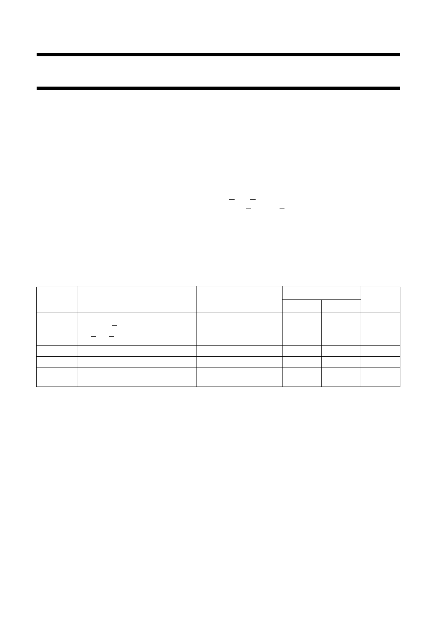
FUNCTION TABLE
See note 1.
Note
1. H = HIGH voltage level;
L = LOW voltage level;
X = don't care.
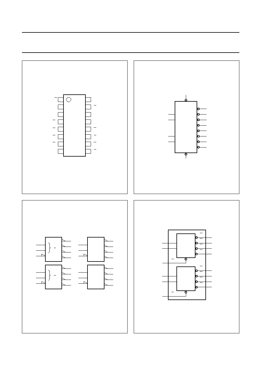
ORDERING INFORMATION
PINNING
INPUTS
OUTPUTS
nE
nA
0
nA
1
nY
0
nY
1
nY
2
nY
3
H
X
X
H
H
H
H
L
L
L
L
H
H
H
L
H
L
H
L
H
H
L
L
H
H
H
L
H
L
H
H
H
H
H
L
OUTSIDE NORTH
AMERICA
NORTH AMERICA
PACKAGES
PINS
PACKAGE
MATERIAL
CODE
74AHC139D
74AHC139D
16
SO
plastic
SOT109-1
74AHC139PW
74AHC139PW DH
16
TSSOP
plastic
SOT403-1
74AHCT139D
74AHCT139D
16
SO
plastic
SOT109-1
74AHCT139PW
74AHCT139PW DH
16
TSSOP
plastic
SOT403-1
PIN
SYMBOL
DESCRIPTION
1 and 15
1E and 2E
enable inputs (active LOW)
2 and 3
1A
0
and 1A
1
address inputs
4, 5, 6 and 7
1Y
0
, 1Y
1
, Y
2
and 1Y
3
outputs (active LOW)
8
GND
ground (0 V)
9, 10, 11 and 12
2Y
3
, 2Y
2
, 2Y
1
and 2Y
0
outputs (active LOW)
13 and 14
2A
1
and 2A
0
address inputs
16
V
CC
DC supply voltage

1999 Sep 01
5
Philips Semiconductors
Product specification
Dual 2-to-4 line decoder/demultiplexer
74AHC139;
74AHCT139
RECOMMENDED OPERATING CONDITIONS
LIMITING VALUES
In accordance with the Absolute Maximum Rating System (IEC 134); voltages are referenced to GND (ground = 0 V).
Notes
1. The input and output voltage ratings may be exceeded if the input and output current ratings are observed.
2. For SO package: above 70
∞
C the value of P
D
derates linearly with 8 mW/K.
For TSSOP package: above 60
∞
C the value of P
D
derates linearly with 5.5 mW/K.
SYMBOL
PARAMETER
CONDITIONS
74AHC
74AHCT
UNIT
MIN.
TYP.
MAX.
MIN.
TYP.
MAX.
V
CC
DC supply voltage
2.0
5.0
5.5
4.5
5.0
5.5
V
V
I
input voltage
0
-
5.5
0
-
5.5
V
V
O
output voltage
0
-
V
CC
0
-
V
CC
V
T
amb
operating ambient
temperature
see DC and AC
characteristics per device
-
40
+25
+85
-
40
+25
+85
∞
C
-
40
+25
+125
-
40
+25
+125
∞
C
t
r
,t
f
(
t/
f)
input rise and fall ratio V
CC
= 3.3
±
0.3 V
-
-
100
-
-
-
ns/V
V
CC
= 5
±
0.5 V
-
-
20
-
-
20
SYMBOL
PARAMETER
CONDITIONS
MIN.
MAX. UNIT
V
CC
DC supply voltage
-
0.5
+7.0
V
V
I
input voltage
-
0.5
+7.0
V
I
IK
DC input diode current
V
I
<
-
0.5 V; note 1
-
-
20
mA
I
OK
DC output diode current
V
O
<
-
0.5 V or V
O
> V
CC
+ 0.5 V; note 1
-
±
20
mA
I
O
DC output source or sink current
-
0.5 V < V
O
< V
CC
+ 0.5 V
-
±
25
mA
I
CC
DC V
CC
or GND current
-
±
75
mA
T
stg
storage temperature
-
65
+150
∞
C
P
D
power dissipation per package
for temperature range:
-
40 to +125
∞
C;
note 2
-
500
mW