2002 Oct 02
2
Philips Semiconductors
Product specification
Buffer with open-drain output
74AHC1G07; 74AHCT1G07
FEATURES
∑
High noise immunity
∑
ESD protection:
≠ HBM EIA/JESD22-A114-A exceeds 2000 V
≠ MM EIA/JESD22-A115-A exceeds 200 V
≠ CDM EIA/JESD22-C101 exceeds 1000 V.
∑
Low power dissipation
∑
SOT353 and SOT753 packages
∑
Output capability standard (open-drain)
∑
Specified from
-
40 to +125
∞
C.
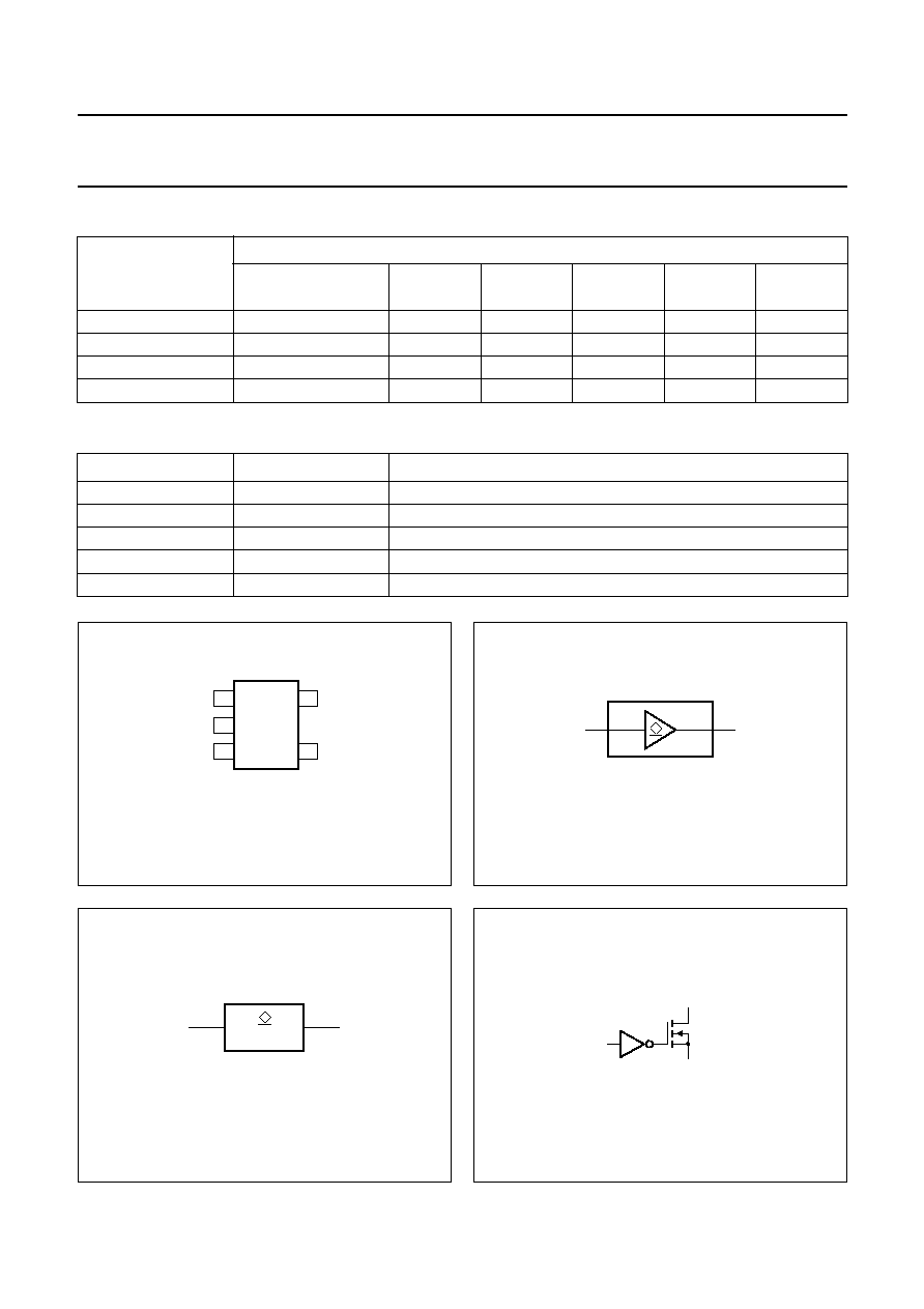
DESCRIPTION
The 74AHC1G/AHCT1G07 is a high-speed Si-gate CMOS
device.
The 74AHC1G/AHCT1G07 provides the non-inverting
buffer.
The output of the 74AHC1G/AHCT1G07 devices is
open-drain and can be connected to other open-drain
outputs to implement active-LOW wired-OR or
active-HIGH wired-AND functions. For digital operation
this device must have a pull-up resistor to establish a logic
HIGH-level.
QUICK REFERENCE DATA
GND = 0 V; T
amb
= 25
∞
C; t
r
= t
f
3.0 ns.
Notes
1. C
PD
is used to determine the dynamic power dissipation (P
D
in
µ
W).
P
D
= C
PD
◊
V
CC
2
◊
f
i
+ (C
L
◊
V
CC
2
◊
f
o
) where:
f
i
= input frequency in MHz;
f
o
= output frequency in MHz;
C
L
= output load capacitance in pF;
V
CC
= supply voltage in Volts.
2. The condition is V
I
= GND to V
CC
.
FUNCTION TABLE
See note 1.
Note
1. H = HIGH voltage level;
L = LOW voltage level;
Z = high-impedance OFF-state.
SYMBOL
PARAMETER
CONDITIONS
TYPICAL
UNIT
AHC1G
AHCT1G
t
PZL
propagation delay A to Y
C
L
= 15 pF; V
CC
= 5 V
2.5
2.8
ns
t
PLZ
propagation delay A to Y
C
L
= 15 pF; V
CC
= 5 V
4.2
3.9
ns
C
I
input capacitance
1.5
1.5
pF
C
PD
power dissipation capacitance
C
L
= 50 pF; f = 1 MHz; notes 1 and 2
5
6.5
pF
INPUT
OUTPUT
A
Y
L
L
H
Z

2002 Oct 02
4
Philips Semiconductors
Product specification
Buffer with open-drain output
74AHC1G07; 74AHCT1G07
RECOMMENDED OPERATING CONDITIONS
LIMITING VALUES
In accordance with the Absolute Maximum Rating System (IEC 60134); voltages are referenced to GND (ground = 0 V).
Note
1. The input and output voltage ratings may be exceeded if the input and output current ratings are observed.
SYMBOL
PARAMETER
CONDITIONS
74AHC
74AHCT
UNIT
MIN.
TYP.
MAX.
MIN.
TYP.
MAX.
V
CC
supply voltage
2.0
5.0
5.5
4.5
5.0
5.5
V
V
I
input voltage
0
-
5.5
0
-
5.5
V
V
O
output voltage
active mode
0
-
V
CC
0
-
V
CC
V
high-impedance mode
0
-
6.0
0
-
6.0
V
T
amb
ambient
temperature
see DC and AC
characteristics per device
-
40
+25
+85
-
40
+25
+85
∞
C
-
40
+25
+125
-
40
+25
+125
∞
C
t
r
, t
f
(
t/
f)
input rise and fall
times ratios
V
CC
= 3.3
±
0.3 V
-
-
100
-
-
-
ns/V
V
CC
= 5
±
0.5 V
-
-
20
-
-
20
ns/V
SYMBOL
PARAMETER
CONDITIONS
MIN.
MAX.
UNIT
V
CC
supply voltage
-
0.5
+7.0
V
V
I
input voltage
-
0.5
+7.0
V
I
IK
input diode current
V
I
<
-
0.5 V; note 1
-
-
20
mA
I
OK
output clamping diode
current
V
O
<
-
0.5 V; note 1
-
±
20
mA
V
O
output voltage
active mode; note 1
-
0.5
+7.0
V
high-impedance mode; note 1
-
0.5
+7.0
V
I
O
output sink current
V
O
>
-
0.5 V
-
±
25
mA
I
CC
V
CC
or GND current
-
±
75
mA
T
stg
storage temperature
-
65
+150
∞
C
P
D
power dissipation per
package
for temperature range from
-
40 to +125
∞
C
-
250
mW

2002 Oct 02
5
Philips Semiconductors
Product specification
Buffer with open-drain output
74AHC1G07; 74AHCT1G07
DC CHARACTERISTICS
74AHC1G family
At recommended operating conditions; voltages are referenced to GND (ground = 0 V).
SYMBOL
PARAMETER
TEST CONDITIONS
T
amb
(
∞
C)
UNIT
OTHER
V
CC
(V)
25
-
40 to +85
-
40 to +125
MIN.
TYP.
MAX.
MIN.
MAX.
MIN.
MAX.
V
IH
HIGH-level input
voltage
2.0
1.5
-
-
1.5
-
1.5
-
V
3.0
2.1
-
-
2.1
-
2.1
-
V
5.5
3.85
-
-
3.85
-
3.85
-
V
V
IL
LOW-level input
voltage
2.0
-
-
0.5
-
0.5
-
0.5
V
3.0
-
-
0.9
-
0.9
-
0.9
V
5.5
-
-
1.65
-
1.65
-
1.65
V
V
OL
LOW-level output
voltage
V
I
= V
IH
or V
IL
;
I
O
= 50
µ
A
2.0
-
0
0.1
-
0.1
-
0.1
V
V
I
= V
IH
or V
IL
;
I
O
= 50
µ
A
3.0
-
0
0.1
-
0.1
-
0.1
V
V
I
= V
IH
or V
IL
;
I
O
= 50
µ
A
4.5
-
0
0.1
-
0.1
-
0.1
V
V
I
= V
IH
or V
IL
;
I
O
= 4.0 mA
3.0
-
-
0.36
-
0.44
-
0.55
V
V
I
= V
IH
or V
IL
;
I
O
= 8.0 mA
4.5
-
-
0.36
-
0.44
-
0.55
V
I
LI
input leakage
current
V
I
= V
CC
or GND
5.5
-
-
0.1
-
1.0
-
2.0
µ
A
I
OZ
3-state output
OFF-state current
V
I
= V
IH
or V
IL
;
V
O
= V
CC
or GND
5.5
-
-
±
0.25
-
±
2.5
-
±
10.0
µ
A
I
CC
quiescent supply
current
V
I
= V
CC
or GND;
I
O
= 0
5.5
-
-
1.0
-
10
-
20
µ
A
C
I
input capacitance
-
1.5
10
-
10
-
10
pF