1999 Jun 16
2
Philips Semiconductors
Product specification
Octal D-type flip-flop; positive edge-trigger; 3-state
74AHC574;
74AHCT574
FEATURES
∑
3-state non-inverting outputs for
bus oriented applications
∑
8-bit positive, edge-triggered
register
∑
ESD protection:
HBM EIA/JESD22-A114-A
exceeds 2000 V
MM EIA/JESD22-A115-A
exceeds 200 V
∑
Independent register and 3-state
buffer operation
∑
Common 3-state output enable
input
∑
Output capability; bus driver
∑
I
CC
category: MSI
∑
For AHC only:
operates with CMOS input levels
∑
For AHCT only:
operates with TTL input levels
∑
Specified from
-
40 to +85 and +125
∞
C.
DESCRIPTION
The 74AHC/AHCT574 are high-speed Si-gate CMOS devices and are pin
compatible with low power Schottky TTL (LSTTL). They are specified in
compliance with JEDEC standard no. 7A.
The 74AHC/AHCT574 are octal D-type flip-flops featuring separate D-type
inputs for each flip-flop and 3-state outputs for bus oriented applications.
A clock (CP) and an output enable (OE) input are common to all flip-flops.
The 8 flip-flops will store the state of their individual D-inputs that meet the
set-up and hold times requirements on the LOW-to-HIGH CP transition.
When OE is LOW the contents of the 8 flip-flops are available at the outputs.
When OE is HIGH, the outputs go to the high-impedance OFF-state. Operation
of the OE input does not affect the state of the flip-flops.
The `574' is functionally identical to the `564', but has non-inverting outputs.
The `574' is functionally identical to the `374', but has a different pinning.
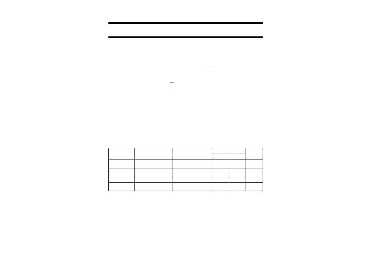
QUICK REFERENCE DATA
GND = 0 V; T
amb
= 25
∞
C; t
r
= t
f
3.0 ns.
Notes
1. C
PD
is used to determine the dynamic power dissipation (P
D
in
µ
W).
P
D
= C
PD
◊
V
CC
2
◊
f
i
+
(C
L
◊
V
CC
2
◊
f
o
) where:
f
i
= input frequency in MHz;
f
o
= output frequency in MHz;
(C
L
◊
V
CC
2
◊
f
o
) = sum of outputs;
C
L
= output load capacitance in pF;
V
CC
= supply voltage in Volts.
2. The condition is V
I
= GND to V
CC
.
SYMBOL
PARAMETER
CONDITIONS
TYPICAL
UNIT
AHC
AHCT
t
PHL
/t
PLH
propagation delay
C
L
= 15 pF; V
CC
= 5 V
4.4
4.4
ns
CP to Q
n
f
max
maximum clock frequency
C
L
= 15 pF; V
CC
= 5 V
130
130
MHz
C
I
input capacitance
V
I
= V
CC
or GND
4.0
4.0
pF
C
O
output capacitance
4.0
4.0
pF
C
PD
power dissipation
capacitance
C
L
= 50 pF; f = 1 MHz;
notes 1 and 2
10
12
pF
1999 Jun 16
3
Philips Semiconductors
Product specification
Octal D-type flip-flop; positive edge-trigger; 3-state
74AHC574;
74AHCT574
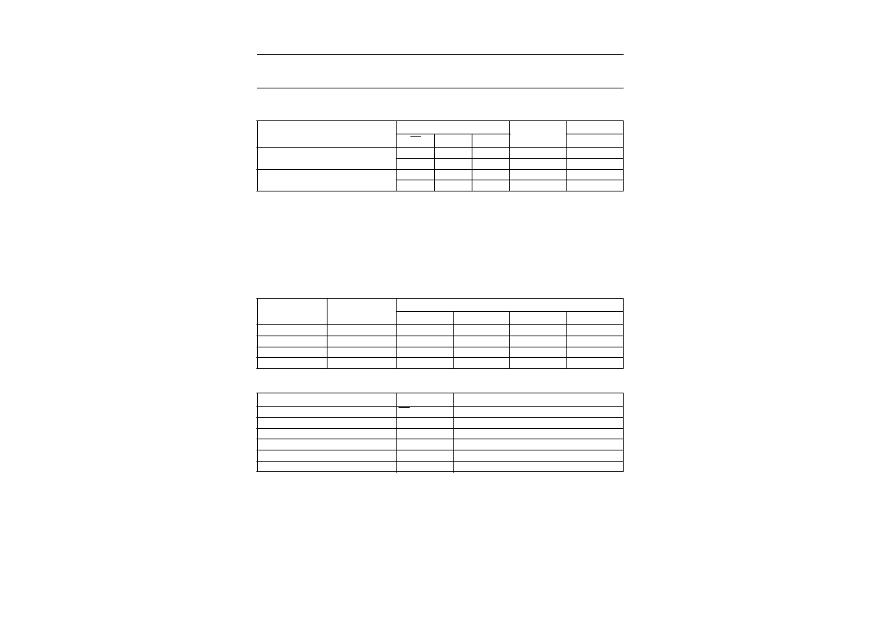
FUNCTION TABLE
See note 1.
Note
1. H = HIGH voltage level;
h = HIGH voltage level one set-up time prior to the LOW-to-HIGH CP transition;
L = LOW voltage level;
I = LOW voltage level one set-up time prior to the LOW-to-HIGH CP transition;
Z = high-impedance OFF-state;
= LOW-to-HIGH CP transition.
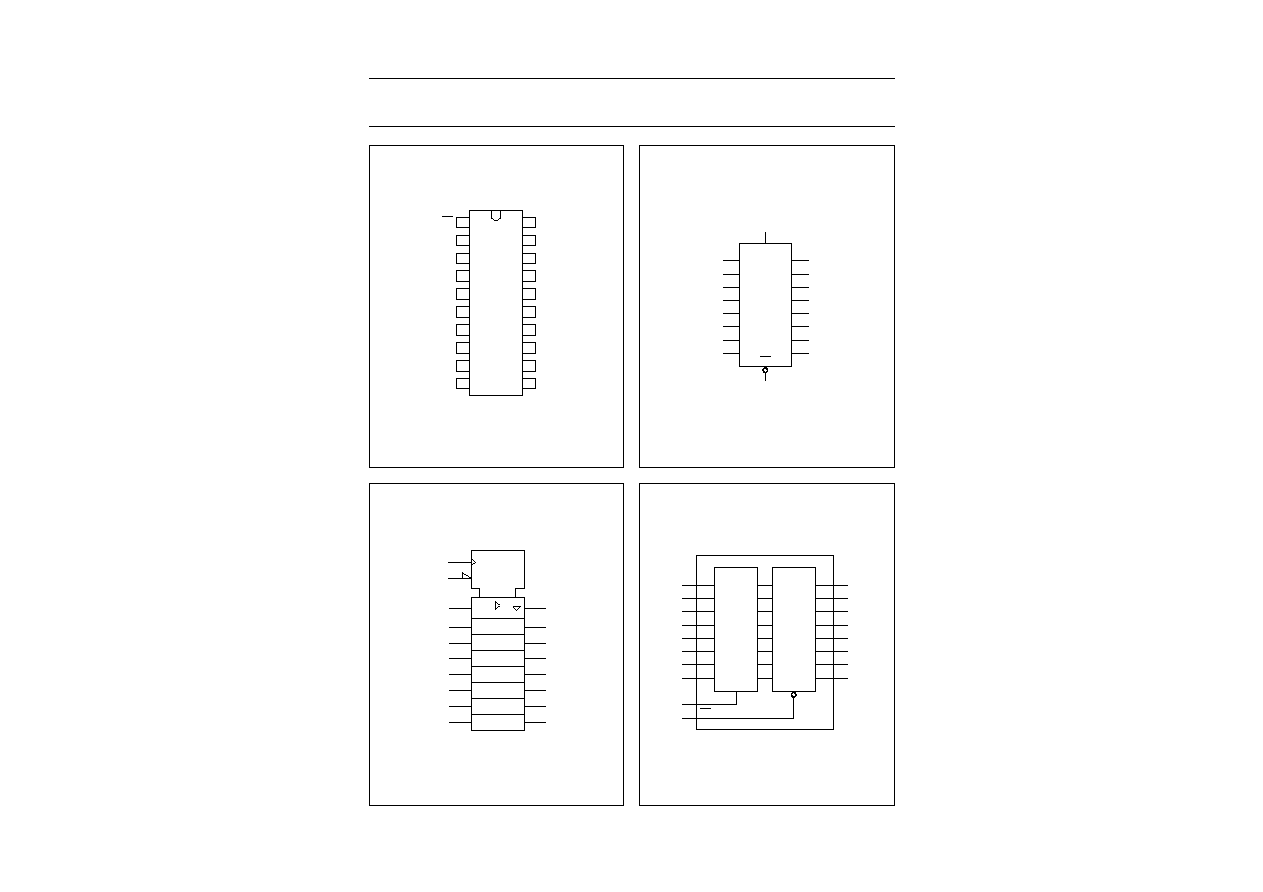
ORDERING INFORMATION
PINNING
OPERATING MODES
INPUTS
INTERNAL
FLIP-FLOPS
OUTPUTS
OE
CP
D
n
Q
0
to Q
7
Load and read register
L
I
L
L
L
h
H
H
Load register and disable outputs
H
l
L
Z
H
h
H
Z
OUTSIDE NORTH
AMERICA
NORTH AMERICA
PACKAGES
PINS
PACKAGE
MATERIAL
CODE
74AHC574D
74AHC574D
20
SO
plastic
SOT163-1
74AHC574PW
74AHC574PW DH
20
TSSOP
plastic
SOT360-1
74AHCT574D
74AHCT574D
20
SO
plastic
SOT163-1
74AHCT574PW
74AHCT574PW DH
20
TSSOP
plastic
SOT360-1
PIN
SYMBOL
DESCRIPTION
1
OE
3-state output enable input (active LOW)
2, 3, 4, 5, 6, 7, 8 and 9
D
0
to D
7
data inputs
10
GND
ground (0 V)
11
CP
clock input (LOW-to-HIGH, edge triggered)
19, 18, 17, 16, 15, 14, 13 and 12
Q
0
to Q
7
3-state flip-flop outputs
20
V
CC
DC supply voltage

1999
Jun
16
5
Philips Semiconductors
Product specification
Octal D-type flip-flop; positive edge-trigger; 3-state
74AHC574;
74AHCT574
This text is here in white to force landscape pages to be rotated correctly when browsing through the pdf in the Acrobat reader.This text is here in
_
white to force landscape pages to be rotated correctly when browsing through the pdf in the Acrobat reader.This text is here inThis text is here in
white to force landscape pages to be rotated correctly when browsing through the pdf in the Acrobat reader. white to force landscape pages to be ...
handbook, full pagewidth
MNA449
Q4
D4
Q3
D3
Q2
D2
Q1
D1
Q0
D0
D
CP
FF1
Q
CP
D
FF2
Q
D
Q
D
Q
D
Q
D
Q
D
Q
D
Q
OE
Q5
D5
Q6
D6
Q7
D7
CP
FF3
CP
FF4
CP
FF5
CP
FF6
CP
FF7
CP
FF8
CP
Fig.5 Logic diagram.