2002 Jun 06
2
Philips Semiconductors
Product specification
Bus buffer/line driver; 3-state
74AHC1G125; 74AHCT1G125
FEATURES
∑
Symmetrical output impedance
∑
High noise immunity
∑
ESD protection:
≠ HBM EIA/JESD22-A114-A exceeds 2000 V
≠ MM EIA/JESD22-A115-A exceeds 200 V
≠ CDM EIA/JESD22-C101 exceeds 1000 V.
∑
Low power dissipation
∑
Balanced propagation delays
∑
Very small 5-pin package
∑
Output capability: standard
∑
Specified from
-
40 to +125
∞
C.
DESCRIPTION
The 74AHC1G/AHCT1G125 is a high-speed Si-gate
CMOS device.
The 74AHC1G/AHCT1G125 provides one non-inverting
buffer/line driver with 3-state output. The 3-state output is
controlled by the output enable input (OE). A HIGH at OE
causes the output to assume a high-impedance
OFF-state.
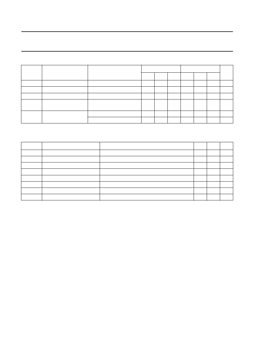
QUICK REFERENCE DATA
GND = 0 V; T
amb
= 25
∞
C; t
r
= t
f
3.0 ns.
Notes
1. C
PD
is used to determine the dynamic power dissipation (P
D
in
µ
W).
P
D
= C
PD
◊
V
CC
2
◊
f
i
+ (C
L
◊
V
CC
2
◊
f
o
) where:
f
i
= input frequency in MHz;
f
o
= output frequency in MHz;
C
L
= output load capacitance in pF;
V
CC
= supply voltage in Volts.
2. The condition is V
I
= GND to V
CC
.
FUNCTION TABLE
See note 1.
Note
1. H = HIGH voltage level;
L = LOW voltage level;
X = don't care;
Z = high-impedance OFF-state.
SYMBOL
PARAMETER
CONDITIONS
TYPICAL
UNIT
AHC1G
AHCT1G
t
PHL
/t
PLH
propagation delay A to Y
C
L
= 15 pF; V
CC
= 5 V
3.4
3.4
ns
C
I
input capacitance
1.5
1.5
pF
C
PD
power dissipation capacitance
C
L
= 50 pF; f = 1 MHz; notes 1 and 2
9
11
pF
INPUTS
OUTPUT
OE
A
Y
L
L
L
L
H
H
H
X
Z
2002 Jun 06
4
Philips Semiconductors
Product specification
Bus buffer/line driver; 3-state
74AHC1G125; 74AHCT1G125
RECOMMENDED OPERATING CONDITIONS
LIMITING VALUES
In accordance with the Absolute Maximum Rating System (IEC 60134); voltages are referenced to GND (ground = 0 V).
Note
1. The input and output voltage ratings may be exceeded if the input and output current ratings are observed.
SYMBOL
PARAMETER
CONDITIONS
74AHC1G
74AHCT1G
UNIT
MIN.
TYP.
MAX.
MIN.
TYP.
MAX.
V
CC
supply voltage
2.0
5.0
5.5
4.5
5.0
5.5
V
V
I
input voltage
0
-
5.5
0
-
5.5
V
V
O
output voltage
0
-
V
CC
0
-
V
CC
V
T
amb
operating ambient
temperature
see DC and AC
characteristics per device
-
40
+25
+125
-
40
+25
+125
∞
C
t
r
, t
f
input rise and fall times
V
CC
= 3.3
±
0.3 V
-
-
100
-
-
-
ns/V
V
CC
= 5
±
0.5 V
-
-
20
-
-
20
ns/V
SYMBOL
PARAMETER
CONDITIONS
MIN.
MAX. UNIT
V
CC
supply voltage
-
0.5
+7.0
V
V
I
input voltage
-
0.5
+7.0
V
I
IK
input diode current
V
I
<
-
0.5 V
-
-
20
mA
I
OK
output diode current
V
O
<
-
0.5 V or V
O
> V
CC
+ 0.5 V; note 1
-
±
20
mA
I
O
output source or sink current
-
0.5 V < V
O
< V
CC
+ 0.5 V
-
±
25
mA
I
CC
V
CC
or GND current
-
±
75
mA
T
stg
storage temperature
-
65
+150
∞
C
P
D
power dissipation per package for temperature range from
-
40 to +125
∞
C
-
250
mW