1999 Nov 23
2
Philips Semiconductors
Product specification
Octal D-type transparent latch; 3-state
74AHC373; 74AHCT373
FEATURES
∑
ESD protection:
HBM EIA/JESD22-A114-A exceeds 2000 V
MM EIA/JESD22-A115-A exceeds 200 V
CDM EIA/JESD22-C101 exceeds 1000 V
∑
Balanced propagation delays
∑
All inputs have Schmitt-trigger actions
∑
Inputs accepts voltages higher than V
CC
∑
Common 3-state output enable input
∑
Functionally identical to the `533', `563' and `573'
∑
For AHC only: operates with CMOS input levels
∑
For AHCT only: operates with TTL input levels
∑
Specified from
-
40 to +85
∞
C and
-
40 to +125
∞
C.
DESCRIPTION
The 74AHC/AHCT373 are high-speed Si-gate CMOS
devices and are pin compatible with Low power Schottky
TTL (LSTTL). They are specified in compliance with
JEDEC standard no. 7A.
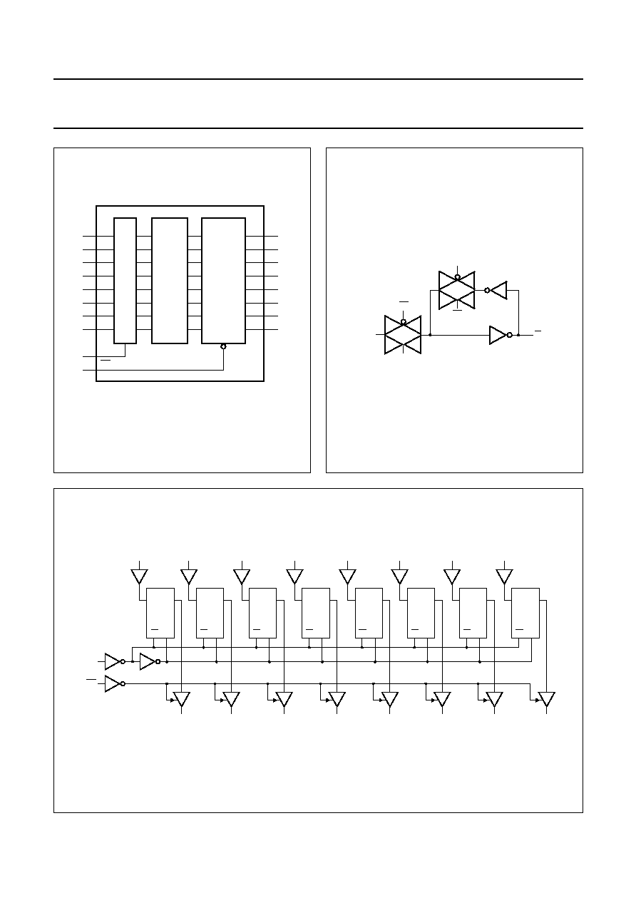
The 74AHC/AHCT373 are octal D-type transparent
latches featuring separate D-type inputs for each latch and
3-state outputs for bus oriented applications. A Latch
Enable (LE) input and an Output Enable (OE) input are
common to all latches.
The `373' consists of eight D-type transparent latches with
3-state true outputs. When LE is HIGH, data at the
D
n
inputs enters the latches. In this condition the latches
are transparent, i.e. a latch output will change state each
time its corresponding D-input changes.
When LE is LOW the latches store the information that
was present at the D-inputs a set-up time preceding the
HIGH-to-LOW transition of LE. When OE is LOW, the
contents of the 8 latches are available at the outputs.
When OE is HIGH, the outputs go to the high-impedance
OFF-state. Operation of the OE input does not affect the
state of the latches.
The `373' is functionally identical to the `533', `563' and
`573', but the `533' and `563' have inverted outputs and the
`563' and `573' have a different pin arrangement.
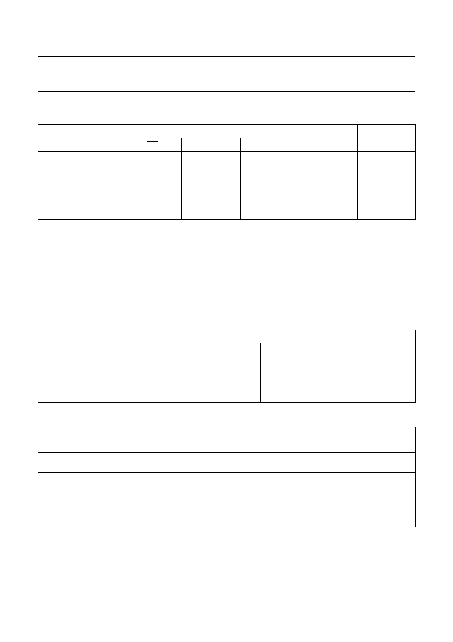
QUICK REFERENCE DATA
Ground = 0 V; T
amb
= 25
∞
C; t
r
= t
f
3.0 ns.
Notes
1. C
PD
is used to determine the dynamic power dissipation (P
D
in
µ
W).
P
D
= C
PD
◊
V
CC
2
◊
f
i
+
(C
L
◊
V
CC
2
◊
f
o
) where:
f
i
= input frequency in MHz;
f
o
= output frequency in MHz;
(C
L
◊
V
CC
2
◊
f
o
) = sum of outputs;
C
L
= output load capacitance in pF;
V
CC
= supply voltage in Volts.
2. The condition is V
I
= GND to V
CC
.
SYMBOL
PARAMETER
CONDITIONS
TYPICAL
UNIT
AHC
AHCT
t
PHL
/t
PLH
propagation delay
D
n
to Q
n
; LE to Q
n
C
L
= 15 pF; V
CC
= 5 V
4.3
4.3
ns
C
I
input capacitance
V
I
= V
CC
or GND
3.0
3.0
pF
C
O
output capacitance
4.0
4.0
pF
C
PD
power dissipation
capacitance
C
L
= 50 pF; f = 1 MHz;
notes 1 and 2
10
12
pF
1999 Nov 23
3
Philips Semiconductors
Product specification
Octal D-type transparent latch; 3-state
74AHC373; 74AHCT373
FUNCTION TABLE
See note 1.
Note
1. H = HIGH voltage level;
h = HIGH voltage level one set-up time prior to the HIGH-to-LOW LE transition;
L = LOW voltage level;
I = LOW voltage level one set-up time prior to the HIGH-to-LOW LE transition;
X = don't care;
Z = high-impedance OFF-state.
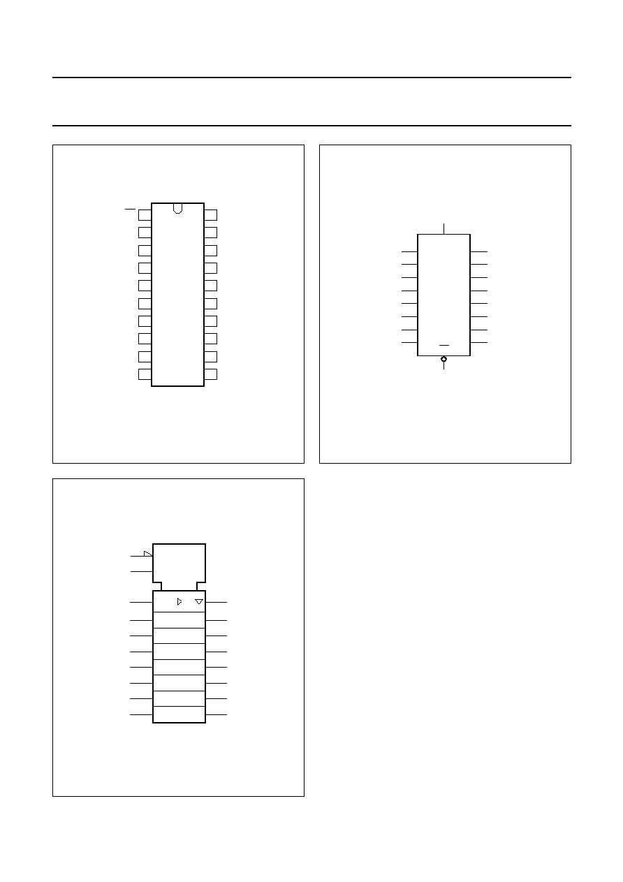
ORDERING INFORMATION
PINNING
OPERATING MODES
INPUTS
INTERNAL
LATCHES
OUTPUTS
OE
LE
D
n
Q
0
to Q
7
Enable and read register
(transparent mode)
L
H
L
L
L
L
H
H
H
H
Latch and read register
L
L
I
L
L
L
L
h
H
H
Latch register and
disable outputs
H
X
X
X
Z
H
X
X
X
Z
OUTSIDE NORTH
AMERICA
NORTH AMERICA
PACKAGES
PINS
PACKAGE
MATERIAL
CODE
74AHC373D
74AHC373D
20
SO
plastic
SOT163-1
74AHC373PW
74AHC373PW DH
20
TSSOP
plastic
SOT360-1
74AHCT373D
74AHCT373D
20
SO
plastic
SOT163-1
74AHCT373PW
7AHCT373PW DH
20
TSSOP
plastic
SOT360-1
PIN
SYMBOL
DESCRIPTION
1
OE
output enable input (active LOW)
2, 5, 6, 9, 12, 15, 16
and 19
Q
0
to Q
7
latch outputs
3, 4, 7, 8, 13, 14, 17
and 18
D
0
to D
7
data inputs
10
GND
ground (0 V)
11
LE
latch enable input (active HIGH)
20
V
CC
DC supply voltage