Philips
Semiconductors
74ALVC16836A
20-bit registered driver with
inverted register enable (3-State)
Product specification
Replaces datasheet 74ALVC16836 of 2000 Jan 04
IC24 Data Handbook
2000 Mar 14
INTEGRATED CIRCUITS
Philips Semiconductors
Product specification
74ALVC16836A
20-bit registered driver with inverted register enable
(3-State)
2
2000 Mar 14
853≠2194 23314
FEATURES
∑
Wide supply voltage range of 1.2 V to 3.6 V
∑
Complies with JEDEC standard no. 8-1A.
∑
CMOS low power consumption
∑
Direct interface with TTL levels
∑
Current drive
±
24 mA at 3.0 V
∑
MULTIBYTE
TM
flow-through standard pin-out architecture
∑
Low inductance multiple V
CC
and GND pins for minimum noise
and ground bounce
∑
Output drive capability 50
transmission lines @ 85
∞
C
∑
Input diodes to accommodate strong drivers
DESCRIPTION
The 74ALVC16836A is a 20-bit universal bus driver. Data flow is
controlled by active low output enable (OE), active low latch enable
(LE) and clock inputs (CP).
When LE is LOW, the A to Y data flow is transparent. When LE is
HIGH and CP is held at LOW or HIGH, the data is latched; on the
LOW to HIGH transient of CP the A-data is stored in the
latch/flip-flop.
When OE is LOW the outputs are active. When OE is HIGH, the
outputs go to the high impedance OFF-state. Operation of the OE
input does not affect the state of the latch/flip-flop.
To ensure the high-impedance state during power up or power
down, OE should be tied to V
CC
through a pullup resistor; the
minimum value of the resistor is determined by the current-sinking
capability of the driver.
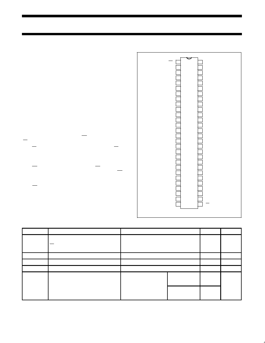
PIN CONFIGURATION
1
2
3
4
5
6
7
8
9
10
11
12
13
14
15
16
17
18
19
20
21
22
23
24
25
26
27
28
29
30
31
32
33
34
35
36
37
38
39
40
41
42
43
44
45
46
47
48
49
50
51
52
53
54
55
56
OE
NC
Y
1
Y
2
Y
3
Y
4
Y
5
GND
V
CC
GND
Y
6
Y
7
Y
8
Y
9
Y
10
Y
11
GND
Y
12
Y
13
Y
14
V
CC
Y
15
Y
16
GND
Y
17
CP
GND
A
1
A
2
V
CC
A
3
A
4
A
5
GND
A
6
A
7
A
8
A
9
A
10
A
11
GND
A
12
A
13
A
14
V
CC
A
15
A
16
GND
A
17
SH00197
Y
18
Y
19
Y
20
LE
A
18
A
19
A
20
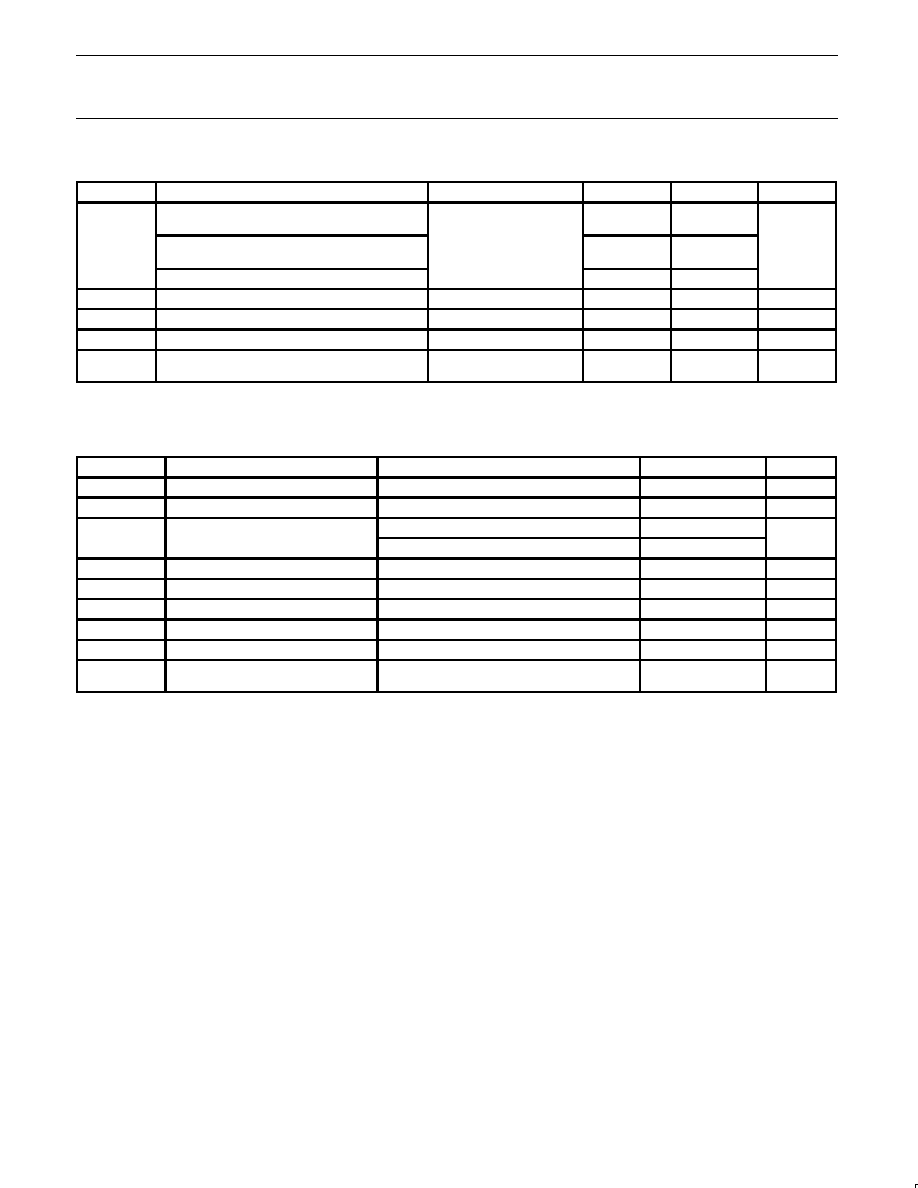
QUICK REFERENCE DATA
GND = 0 V; T
amb
= 25
∞
C; t
r
= t
f
2.5 ns
SYMBOL
PARAMETER
CONDITIONS
TYPICAL
UNIT
t
PHL
/t
PLH
Propagation delay
An to Yn;
LE to Yn;
CP to Yn
V
CC
= 3.3 V, C
L
= 50 pF
2.3
2.6
2.5
ns
f
max
Maximum clock frequency
V
CC
= 3.3 V, C
L
= 50 pF
350
MHz
C
I
Input capacitance
4.0
pF
C
I/O
Input/Output capacitance
8.0
pF
C
Power dissipation capacitance per buffer
V = GND to V
CC
1
transparent mode
Output enabled
Output disabled
13
3
pF
C
PD
Power dissipation capacitance per buffer
V
I
= GND to V
CC
1
Clocked mode
Output enabled
Output disabled
22
15
pF
NOTES:
1. C
PD
is used to determine the dynamic power dissipation (P
D
in
µ
W):
P
D
= C
PD
◊
V
CC
2
◊
f
i
+
S
(C
L
◊
V
CC
2
◊
f
o
) where: f
i
= input frequency in MHz; C
L
= output load capacitance in pF;
f
o
= output frequency in MHz; V
CC
= supply voltage in V;
S
(C
L
◊
V
CC
2
◊
f
o
) = sum of outputs.
Philips Semiconductors
Product specification
74ALVC16836A
20-bit registered driver with inverted register enable
(3-State)
2000 Mar 14
3
ORDERING INFORMATION
PACKAGES
TEMPERATURE
RANGE
ORDER CODE
DRAWING
NUMBER
56-Pin Plastic Thin Shrink Small Outline (TSSOP) Type II
≠40
∞
C to +85
∞
C
74ALVC16836A DGG
SOT364-1
PIN DESCRIPTION
PIN NUMBER
SYMBOL
NAME AND FUNCTION
28
NC
No connection
2, 3, 5, 6, 8, 9, 10, 12,
13, 14, 15, 16, 17, 19,
20, 21, 23, 24, 26, 27
Y
1
to Y
18
Data outputs
4, 11, 18, 25, 32, 39, 46,
53, 56
GND
Ground (0 V)
7, 22, 35, 50
V
CC
Positive supply voltage
1
OE
Output enable input
(active LOW)
29
LE
Latch enable input
(active LOW)
56
CP
Clock input
55, 54, 52, 51, 49, 48,
47, 45, 44, 43, 42, 41,
40, 38, 37, 36, 34, 33,
31, 30
A
1
to A
18
Data inputs
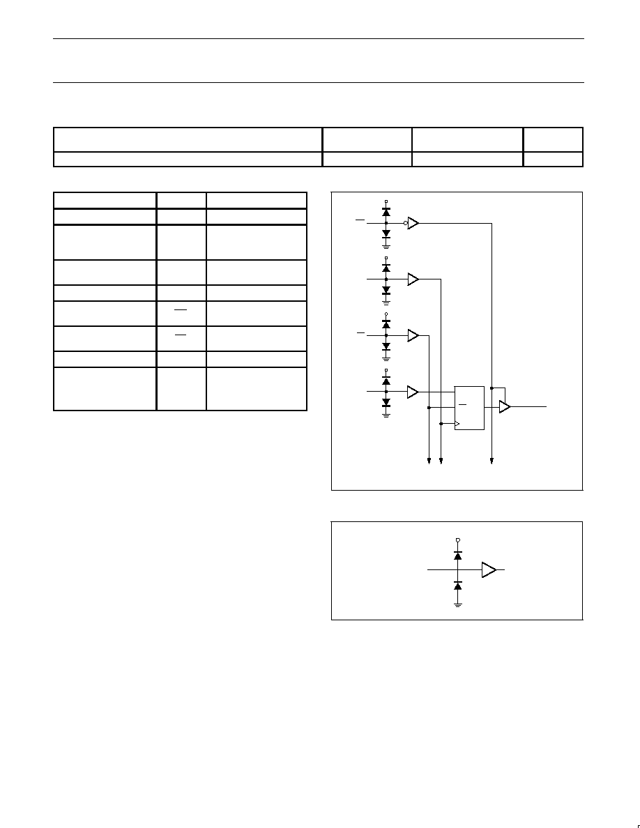
LOGIC SYMBOL
SH00202
CP
LE
D
OE
LE
A
1
Y
1
TO THE 17 OTHER CHANNELS
CP
TYPICAL INPUT (DATA OR CONTROL)
SH00200
A1
V
CC
Philips Semiconductors
Product specification
74ALVC16836A
20-bit registered driver with inverted register enable
(3-State)
2000 Mar 14
4
LOGIC SYMBOL (IEEE/IEC)
1
1
30
28
54
52
51
49
48
47
45
44
43
42
41
40
38
37
36
34
33
31
3
5
6
8
9
10
12
13
14
15
16
17
19
20
21
23
24
26
3D
27
2C3
EN1
A
1
A
2
A
3
A
4
A
5
A
6
A
7
A
8
A
9
A
10
A
11
A
12
A
13
A
14
A
15
A
16
A
17
A
18
OE
CP
Y
1
Y
2
Y
3
Y
4
Y
5
Y
6
Y
7
Y
8
Y
9
Y
10
Y
11
Y
12
Y
13
Y
14
Y
15
Y
16
Y
17
Y
18
LE
C3
G2
SH00196
FUNCTION TABLE
INPUTS
OUTPUTS
OE
LE
CP
A
OUTPUTS
H
X
X
X
Z
L
L
X
L
L
L
L
X
H
H
L
H
L
L
L
H
H
H
L
H
H
X
Y
0
1
L
H
L
X
Y
0
2
H
=
HIGH voltage level
L
=
LOW voltage level
X
=
Don't care
Z
=
High impedance "off" state
=
LOW-to-HIGH level transition
NOTES:
1. Output level before the indicated steady-state input conditions
were established, provided that CP is high before LE goes low.
2. Output level before the indicated steady-state input conditions
were established.
Philips Semiconductors
Product specification
74ALVC16836A
20-bit registered driver with inverted register enable
(3-State)
2000 Mar 14
5
RECOMMENDED OPERATING CONDITIONS
SYMBOL
PARAMETER
CONDITIONS
MIN
MAX
UNIT
DC supply voltage 2.5 V range (for max. speed
performance @ 30 pF output load)
2.3
2.7
V
CC
DC supply voltage 3.3 V range (for max. speed
performance @ 50 pF output load)
3.0
3.6
V
DC supply voltage (for low-voltage applications)
1.2
3.6
V
I
DC Input voltage range
0
V
CC
V
V
O
DC output voltage range
0
V
CC
V
T
amb
Operating free-air temperature range
≠40
+85
∞
C
t
r
, t
f
Input rise and fall times
V
CC
= 2.3 to 3.0 V
V
CC
= 3.0 to 3.6 V
0
0
20
10
ns/V
ABSOLUTE MAXIMUM RATINGS
In accordance with the Absolute Maximum Rating System (IEC 134).
Voltages are referenced to GND (ground = 0 V).
SYMBOL
PARAMETER
CONDITIONS
RATING
UNIT
V
CC
DC supply voltage
≠0.5 to +4.6
V
I
IK
DC input diode current
V
I
t
0
≠50
mA
V
DC input voltage
For control pins
1
≠0.5 to +4.6
V
V
I
DC input voltage
For data inputs
1
≠0.5 to V
CC
+0.5
V
I
OK
DC output diode current
V
O
u
V
CC
or V
O
t
0
"
50
mA
V
O
DC output voltage
Note 1
≠0.5 to V
CC
+0.5
V
I
O
DC output source or sink current
V
O
= 0 to V
CC
"
50
mA
I
GND
, I
CC
DC V
CC
or GND current
"
100
mA
T
stg
Storage temperature range
≠65 to +150
∞
C
P
TOT
Power dissipation per package
≠plastic thin-medium-shrink (TSSOP)
For temperature range: ≠40 to +125
∞
C
above +55
∞
C derate linearly with 8 mW/K
600
mW
NOTE:
1. The input and output voltage ratings may be exceeded if the input and output current ratings are observed.