Philips
Semiconductors
74ALVC16244/74ALVCH16244
2.5V/3.3V 16-bit buffer/line driver (3-State)
Product specification
Supersedes data of 1997 Mar 21
IC24 Data Handbook
1998 Jun 29
INTEGRATED CIRCUITS
Philips Semiconductors
Product specification
74ALVC16244/
74ALVCH16244
16-bit buffer/line driver (3-State)
2
1998 Jun 29
853-2082 19638
FEATURES
∑
Wide supply voltage range of 1.2V to 3.6V
∑
Complies with JEDEC standard no. 8-1A
∑
CMOS low power consumption
∑
MULTIBYTE
TM
flow-through standard pin-out architecture
∑
Low inductance multiple V
CC
and GND pins for minimum noise
and ground bounce
∑
Direct interface with TTL levels
∑
Bus hold on data inputs (74ALVCH16244 only)
∑
Output drive capability 50
transmission lines @ 85
∞
C
∑
Current drive
±
24 mA at 3.0 V
DESCRIPTION
The 74ALVC16244(74ALVCH16244) is a 16-bit non-inverting
buffer/line driver with 3-State outputs. The device can be used as
four 4-bit buffers, two 8-bit buffers or one 16-bit buffer. The 3-State
outputs are controlled by the output enable inputs 1OE and 2OE. A
HIGH on nOE causes the outputs to assume a high impedance
OFF-state.
The 74ALVCH16244 has active bus hold circuitry which is provided
to hold unused or floating data inputs at a valid logic level. This
feature eliminates the need for external pull-up or pull-down
resistors.
The 74ALVC16244 has 5V tolerant inputs.
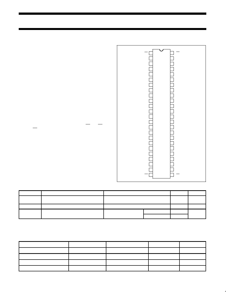
PIN CONFIGURATION
1
2
3
4
5
6
7
8
9
10
11
12
13
14
15
16
17
18
19
20
29
30
31
32
33
34
35
36
37
38
39
40
41
42
43
44
45
46
47
48
1OE
1Y0
1Y1
GND
1Y2
1Y3
V
CC
2Y1
GND
2Y2
2Y3
3Y0
3Y1
GND
2Y0
3Y2
3Y3
V
CC
4Y0
4Y1
4A1
4A0
V
CC
3A3
3A2
GND
3A1
3A0
2A3
2A2
GND
2A1
2A0
V
CC
1A3
1A2
GND
1A1
1A0
2OE
21
22
23
24
25
26
27
28
GND
4Y2
4Y3
4OE
3OE
4A3
4A2
GND
SW00194
QUICK REFERENCE DATA
GND = 0 V; T
amb
= 25
∞
C; t
r
= t
f
2.5 ns
SYMBOL
PARAMETER
CONDITIONS
TYPICAL
UNIT
t
PHL
/t
PLH
Propagation delay
An to Yn
V
CC
= 2.5V, CL = 30pF
V
CC
= 3.3V, CL = 50pF
1.9
1.9
ns
C
I
Input capacitance
5.0
pF
C
Power dissipation capacitance per buffer
V = GND to V
CC
1
Outputs enabled
25
pF
C
PD
Power dissipation capacitance per buffer
V
I
= GND to V
CC
1
Outputs disabled
4
pF
NOTE:
1. C
PD
is used to determine the dynamic power dissipation (P
D
in
m
W):
P
D
= C
PD
◊
V
CC
2
◊
f
i
+
S
(C
L
◊
V
CC
2
◊
f
o
) where: f
i
= input frequency in MHz; C
L
= output load capacitance in pF;
f
o
= output frequency in MHz; V
CC
= supply voltage in V;
S
(C
L
◊
V
CC
2
◊
f
o
) = sum of the outputs.
ORDERING INFORMATION
PACKAGES
TEMPERATURE RANGE
OUTSIDE NORTH AMERICA
NORTH AMERICA
DWG NUMBER
48-Pin Plastic SSOP Type III
≠40
∞
C to +85
∞
C
74ALVC16244 DL
AC16244 DL
SOT370-1
48-Pin Plastic TSSOP Type II
≠40
∞
C to +85
∞
C
74ALVC16244 DGG
AC16244 DGG
SOT362-1
48-Pin Plastic SSOP Type III
≠40
∞
C to +85
∞
C
74ALVCH16244 DL
ACH16244 DL
SOT370-1
48-Pin Plastic TSSOP Type II
≠40
∞
C to +85
∞
C
74ALVCH16244 DGG
ACH16244 DGG
SOT362-1
Philips Semiconductors
Product specification
74ALVC16244/
74ALVCH16244
16-bit buffer/line driver (3-State)
1998 Jun 29
3
PIN DESCRIPTION
PIN NUMBER
SYMBOL
NAME AND FUNCTION
1
1OE
Output enable input
(active LOW)
2, 3, 5, 6
1Y0 to 1Y3
Data outputs
4, 10, 15, 21,
28, 34, 39, 45
GND
Ground (0V)
7, 18, 31, 42
V
CC
Positive supply voltage
8, 9, 11, 12
2Y0 to 2Y3
Data outputs
13, 14, 16, 17
3Y0 to 3Y3
Data outputs
19, 20, 22, 23
4Y0 to 4Y3
Data outputs
24
4OE
Output enable input
(active LOW)
25
3OE
Output enable input
(active LOW)
30, 29, 27, 26
4A0 to 4A3
Data inputs
36, 35, 33, 32
3A0 to 3A3
Data inputs
41, 40, 38, 37
2A0 to 2A3
Data inputs
47, 46, 44, 43
1A0 to 1A3
Data inputs
48
2OE
Output enable input
(active LOW)
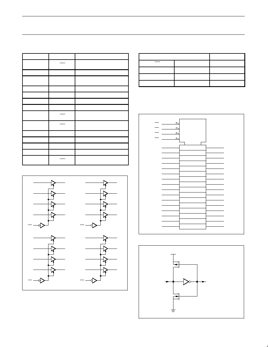
LOGIC SYMBOL
47
46
44
43
1
2
3
5
6
1A0
1A1
1A2
1A3
1OE
1Y0
1Y1
1Y2
1Y3
36
35
33
32
25
13
14
16
17
3A0
3A1
3A2
3A3
3OE
3Y0
3Y1
3Y2
3Y3
41
40
38
37
48
8
9
11
12
2A0
2A1
2A2
2A3
2OE
2Y0
2Y1
2Y2
2Y3
30
29
27
26
24
19
20
22
23
4A0
4A1
4A2
4A3
4OE
4Y0
4Y1
4Y2
4Y3
SW00195
FUNCTION TABLE
INPUTS
OUTPUT
nOE
nAn
nYn
L
L
L
L
H
H
H
X
Z
H = HIGH voltage level
L = LOW voltage level
X = don't care
Z = high impedance OFF-state
LOGIC SYMBOL (IEEE/IEC)
SW00056
48
1EN
1
46
44
43
41
40
38
37
36
2EN
3EN
4EN
2
3
4
1
25
24
47
35
33
32
30
29
27
26
3
2
5
6
8
9
11
12
13
14
16
17
19
20
22
23
1OE
2OE
3OE
4OE
1A0
1A1
1A2
1A3
2A0
2A1
2A2
3A0
3A1
3A2
3A3
4A0
4A1
4A2
4A3
1Y0
1Y1
1Y2
1Y3
2Y0
2Y1
2Y2
2Y3
3Y0
3Y1
3Y2
3Y3
4Y0
4Y3
2A3
4Y1
4Y2
1
1
1
1
BUS HOLD CIRCUIT
To internal circuit
V
CC
Data Input
SW00044
Philips Semiconductors
Product specification
74ALVC16244/
74ALVCH16244
16-bit buffer/line driver (3-State)
1998 Jun 29
4
RECOMMENDED OPERATING CONDITIONS
SYMBOL
PARAMETER
CONDITIONS
LIMITS
UNIT
SYMBOL
PARAMETER
CONDITIONS
MIN
MAX
UNIT
DC supply voltage 2.5V range (for max. speed
performance @ 30 pF output load)
2.3
2.7
V
CC
DC supply voltage 3.3V range (for max. speed
performance @ 50 pF output load)
3.0
3.6
V
DC supply voltage (for low-voltage applications)
1.2
3.6
For data input pins with
bus hold
0
V
CC
V
I
DC Input voltage range
For data input pins without
bus hold
0
5.5
V
For control pins
0
5.5
V
O
DC output voltage range
0
V
CC
V
T
amb
Operating free-air temperature range
≠40
+85
∞
C
t
r
, t
f
Input rise and fall times
V
CC
= 2.3 to 3.0V
V
CC
= 3.0 to 3.6V
0
0
20
10
ns/V
ABSOLUTE MAXIMUM RATINGS
1
In accordance with the Absolute Maximum Rating System (IEC 134)
Voltages are referenced to GND (ground = 0V)
SYMBOL
PARAMETER
CONDITIONS
RATING
UNIT
V
CC
DC supply voltage
≠0.5 to +4.6
V
I
IK
DC input diode current
V
I
t
0
≠50
mA
For data inputs with bus hold
2
≠0.5 to V
CC
+0.5
V
I
DC input voltage
For data inputs without bus hold
2
≠0.5 to +5.5
V
For control pins
2
≠0.5 to +5.5
I
OK
DC output diode current
V
O
u
V
CC
or V
O
t
0
"
50
mA
V
O
DC output voltage
Note 2
≠0.5 to V
CC
+0.5
V
I
O
DC output source or sink current
V
O
= 0 to V
CC
"
50
mA
I
GND
, I
CC
DC V
CC
or GND current
"
100
mA
T
stg
Storage temperature range
≠65 to +150
∞
C
P
TOT
Power dissipation per package
≠plastic medium-shrink (SSOP)
≠plastic thin-medium-shrink (TSSOP)
For temperature range: ≠40 to +125
∞
C
above +55
∞
C derate linearly with 11.3 mW/K
above +55
∞
C derate linearly with 8 mW/K
850
600
mW
NOTES:
1. Stresses beyond those listed may cause permanent damage to the device. These are stress ratings only and functional operation of the
device at these or any other conditions beyond those indicated under "recommended operating conditions" is not implied. Exposure to
absolute-maximum-rated conditions for extended periods may affect device reliability.
2. The input and output voltage ratings may be exceeded if the input and output current ratings are observed.
Philips Semiconductors
Product specification
74ALVC16244/
74ALVCH16244
16-bit buffer/line driver (3-State)
1998 Jun 29
5
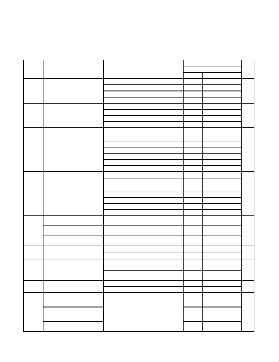
DC CHARACTERISTICS
Over recommended operating conditions. Voltage are referenced to GND (ground = 0 V).
LIMITS
SYMBOL
PARAMETER
TEST CONDITIONS
Temp = -40
∞
C to +85
∞
C
UNIT
MIN
TYP
1
MAX
V
CC
= 1.2V
V
CC
V
IH
HIGH level Input voltage
V
CC
= 1.8V
0.7*V
CC
0.9
V
V
IH
HIGH level In ut voltage
V
CC
= 2.3 to 2.7V
1.7
1.2
V
V
CC
= 2.7 to 3.6V
2.0
1.5
V
CC
= 1.2V
GND
V
IL
LOW level Input voltage
V
CC
= 1.8V
0.9
0.2*V
CC
V
V
IL
LOW level In ut voltage
V
CC
= 2.3 to 2.7V
1.2
0.7
V
V
CC
= 2.7 to 3.6V
1.5
0.8
V
CC
= 1 8 to 3 6V; V
I
= V
IH
or V
IL
; I
O
= ≠100
µ
A
V
CC
≠0 2
V
CC
V
CC
= 1.8 to 3.6V; V
I
= V
IH
or V
IL
; I
O
= ≠100
µ
A
V
CC
≠0.2
V
CC
V
CC
= 1.8V; V
I
= V
IH
or V
IL
; I
O
= ≠6mA
V
CC
≠0.4
V
CC
≠0.10
V
CC
= 2.3V; V
I
= V
IH
or V
IL
; I
O
= ≠6mA
V
CC
≠0.3
V
CC
≠0.08
V
OH
HIGH level output voltage
V
CC
= 2.3V; V
I
= V
IH
or V
IL
; I
O
= ≠12mA
V
CC
≠0.5
V
CC
≠0.17
V
V
CC
= 2.3V; V
I
= V
IH
or V
IL
; I
O
= ≠18mA
V
CC
≠0.6
V
CC
≠0.26
V
CC
= 2.7V; V
I
= V
IH
or V
IL
; I
O
= ≠12mA
V
CC
≠0.5
V
CC
≠0.14
V
CC
= 3.0V; V
I
= V
IH
or V
IL;
I
O
= ≠24mA
V
CC
≠1.0
V
CC
≠0.28
V
CC
= 1 8 to 3 6V; V
I
= V
IH
or V
IL
; I
O
= 100
µ
A
GND
0 20
V
CC
= 1.8 to 3.6V; V
I
= V
IH
or V
IL
; I
O
= 100
µ
A
GND
0.20
V
CC
= 1.8V; V
I
= V
IH
or V
IL
; I
O
= 6mA
0.09
0.30
V
CC
= 2.3V; V
I
= V
IH
or V
IL
; I
O
= 6mA
0.07
0.20
V
OL
LOW level output voltage
V
CC
= 2.3V; V
I
= V
IH
or V
IL
; I
O
= 12mA
0.15
0.40
V
V
CC
= 2.3V; V
I
= V
IH
or V
IL
; I
O
= 18mA
0.23
0.60
V
CC
= 2.7V; V
I
= V
IH
or V
IL
; I
O
= 12mA
0.14
0.40
V
CC
= 3.0V; V
I
= V
IH
or V
IL;
I
O
= 24mA
0.27
0.55
Input leakage current per data pin
with bus hold
V
CC
= 1.8 to 3.6V;
V
I
= V
CC
or GND
0.1
5
I
I
Input leakage current per data pin
without bus hold
V
CC
= 1.8 to 3.6V;
V
I
= 5.5 V or GND
0.1
5
µ
A
Input leakage current per control
pin
V
CC
= 1.8 to 3.6V;
V
I
= 5.5 V or GND
0.1
5
I
/I
Input current for common I/O pins
V
CC
= 1.8 to 2.7V; V
I
= V
CC
or GND
0.1
10
µ
A
I
IHZ
/I
ILZ
Input current for common I/O pins
V
CC
= 3.6V; V
I
= V
CC
or GND
0.1
15
µ
A
I
OZ
3-State output OFF-state current
V
CC
= 1.8 to 2.7V; V
I
= V
IH
or V
IL
;
V
O
= V
CC
or GND
0.1
5
µ
A
I
OZ
3-State out ut OFF-state current
V
CC
= 2.7 to 3.6V; V
I
= V
IH
or V
IL
;
V
O
= V
CC
or GND
0.1
10
µ
A
I
CC
Quiescent supply current
V
CC
= 1.8 to 2.7V; V
I
= V
CC
or GND; I
O
= 0
0.1
20
µ
A
I
CC
Quiescent su
ly current
V
CC
= 2.3 to 3.6V; V
I
= V
CC
or GND; I
O
= 0
0.2
40
µ
A
Additional quiescent supply current
given per data I/O pin with bus
hold
150
750
I
CC
Additional quiescent supply current
given per data I/O pin without bus
hold
V
CC
= 2.7V to 3.6V; V
I
= V
CC
≠ 0.6V; I
O
= 0
5
500
µ
A
Additional quiescent supply current
given per control pin
5
500