1999 Oct 14
2
Philips Semiconductors
Product specification
18-bit universal bus transceiver with 30
termination resistor; 3-state
74ALVCH162601
FEATURES
∑
Complies with JEDEC standard
no. 8-1A
∑
CMOS low power consumption
∑
Direct interface with TTL levels
∑
MULTIBYTE
TM
flow-through
standard pin-out architecture
∑
Low inductance multiple V
CC
and
ground pins for minimum noise and
ground bounce
∑
All data inputs have bus hold
circuitry
∑
Integrated 30
termination
resistors.
DESCRIPTION
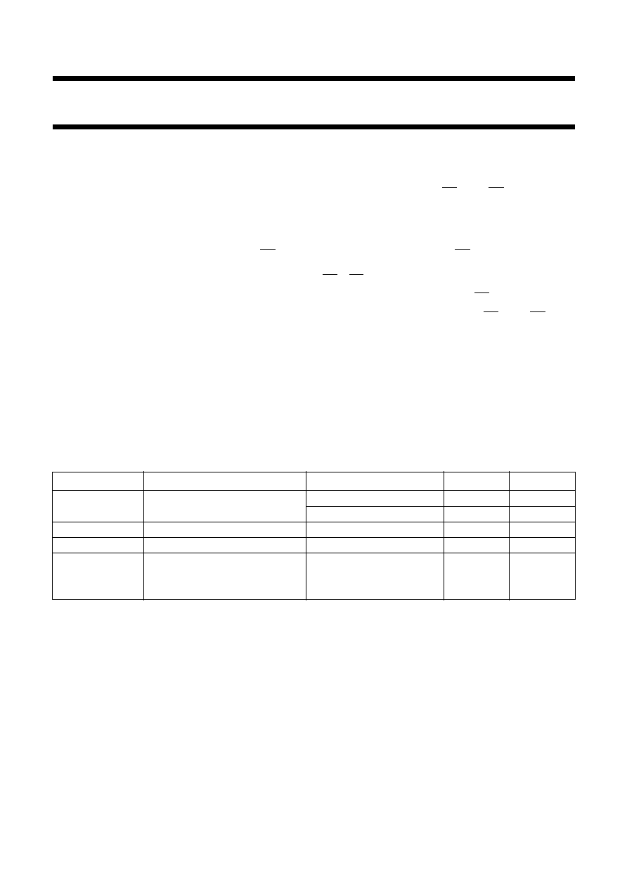
The 74ALVCH162601 is an 18-bit universal transceiver featuring non-inverting
3-state bus compatible outputs in both send and receive directions. Data flow
in each direction is controlled by output enable (OE
AB
and OE
BA
), and clock
(CP
AB
and CP
BA
) inputs. For A-to-B data flow, the device operates in the
transparent mode when LE
AB
is HIGH. When LE
AB
is LOW, the A data is
latched if CP
AB
is held at a HIGH or LOW logic level. If LE
AB
is LOW, the A-bus
data is stored in the latch/flip-flop on the LOW-to-HIGH transition of CP
AB
.
When OE
AB
is LOW, the outputs are active. When OE
AB
is HIGH, the outputs
are in the high-impedance state. The clocks can be controlled with the
clock-enable inputs (CE
BA
/CE
AB
).
Data flow for B-to-A is similar to that of A-to-B but uses OE
BA
, LE
BA
and CP
BA
.
To ensure the high-impedance state during power-down, OE
BA
and OE
AB
should be tied to V
CC
through a pull-up resistor, the minimum value of the
resistor is determined by the current-sinking/current-sourcing capability of the
driver.
The 74ALVCH162601 is designed with 30
series resistors in both HIGH or
LOW output stage.
Active bus hold circuitry is provided to hold unused or floating data inputs at
a valid logic level.
QUICK REFERENCE DATA
Ground = 0; T
amb
= 25
∞
C; t
r
= t
f
= 2.5 ns.
Notes
1. C
PD
is used to determine the dynamic power dissipation (P
D
in
µ
W).
P
D
= C
PD
◊
V
CC
2
◊
f
i
+
(C
L
◊
V
CC
2
◊
f
o
) where:
f
i
= input frequency in MHz;
f
o
= output frequency in MHz;
(C
L
◊
V
CC
2
◊
f
o
) = sum of outputs;
C
L
= output load capacitance in pF;
V
CC
= supply voltage in Volts.
2. The condition is V
I
= GND to V
CC
.
SYMBOL
PARAMETER
CONDITIONS
TYPICAL
UNIT
t
PHL
/t
PLH
propagation delay A
n
, B
n
to B
n
, A
n
C
L
= 30 pF; V
CC
= 2.5 V
4.0
ns
C
L
= 50 pF; V
CC
= 3.3 V
3.1
ns
C
I/O
input/output capacitance
8.0
pF
C
I
input capacitance
4.0
pF
C
PD
power dissipation capacitance per
latch
notes 1 and 2
outputs enabled
21
pF
outputs disabled
3
pF

1999 Oct 14
3
Philips Semiconductors
Product specification
18-bit universal bus transceiver with 30
termination resistor; 3-state
74ALVCH162601
FUNCTION TABLE
See note 1.
Note
1. XX = AB for A-to-B direction, BA for B-to-A direction;
H = HIGH voltage level;
L = LOW voltage level;
h = HIGH state must be present one set-up time before the LOW-to-HIGH transition of CP
XX
;
l = LOW state must be present one set-up time before the LOW-to-HIGH transition of CP
XX
;
X = don't care;
= LOW-to-HIGH level transition;
NC = no change;
Z = high-impedance OFF-state.
ORDERING INFORMATION
INPUTS
OUTPUTS
STATUS
CE
XX
OE
XX
LE
XX
CP
XX
A
n
, B
n
X
H
X
X
X
Z
disabled
X
X
L
L
H
H
X
X
H
L
H
L
transparent
H
L
L
X
X
NC
hold
L
L
L
L
L
L
h
l
H
L
clock and display
L
L
L
L
L
L
L
H
X
X
NC
hold
TYPE NUMBER
PACKAGE
TEMPERATURE RANGE
PINS
PACKAGE
MATERIAL
CODE
74ALVCH162601DGG
-
40 to +85
∞
C
56
TSSOP
plastic
SOT364-1

1999 Oct 14
4
Philips Semiconductors
Product specification
18-bit universal bus transceiver with 30
termination resistor; 3-state
74ALVCH162601
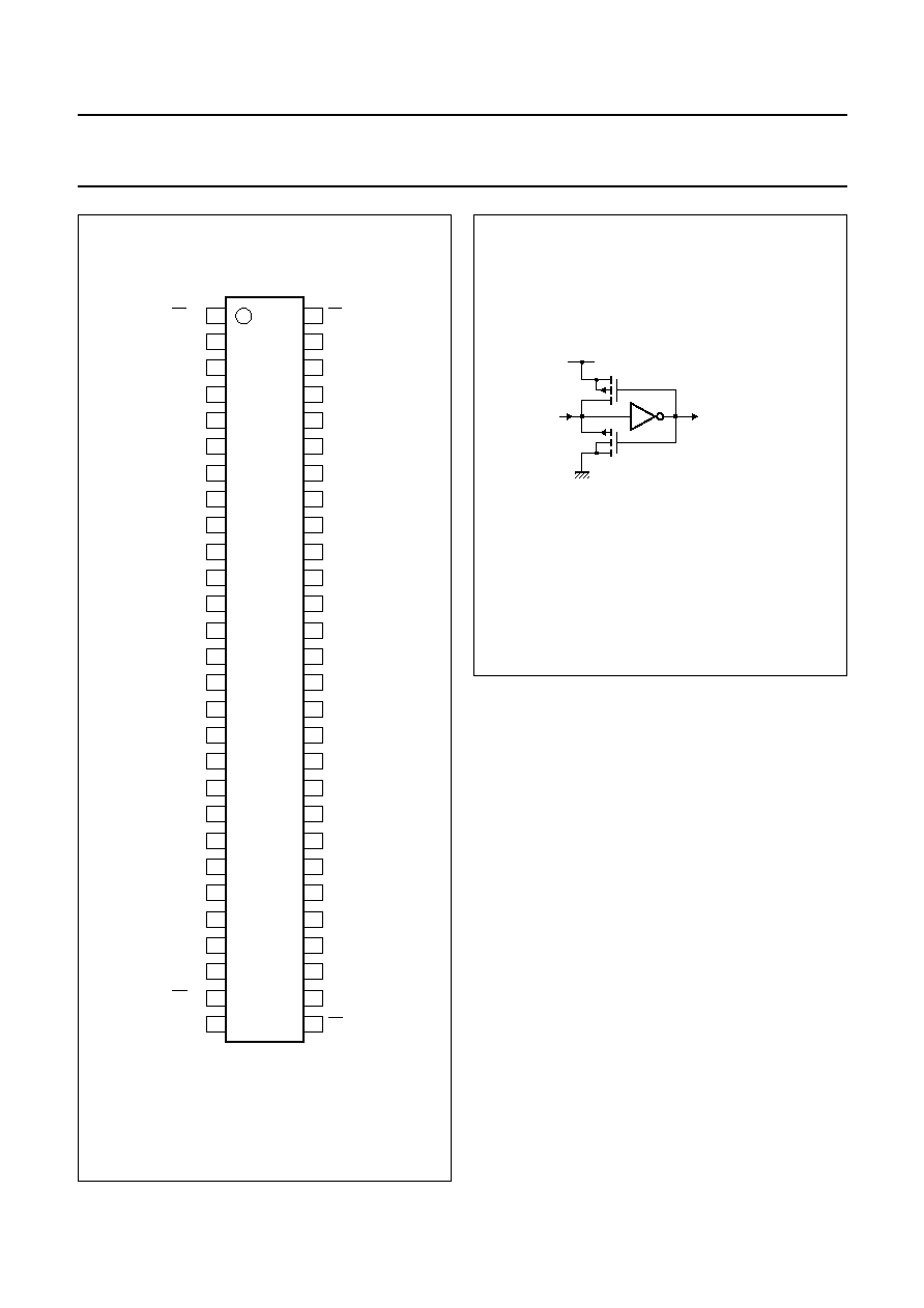
PINNING
PIN
SYMBOL
DESCRIPTION
1
OE
AB
output enable A-to-B
2
LE
AB
latch enable A-to-B
3, 5, 6, 8, 9, 10, 12, 13, 14, 15,
16, 17, 19, 20, 21, 23, 24, 26
A
0
to A
17
data inputs/outputs
4, 11, 18, 25, 32, 39, 46, 53
GND
ground (0 V)
7, 22, 35, 50
V
CC
DC supply voltage
27
OE
BA
output enable B-to-A
28
LE
BA
latch enable B-to-A
29
CE
BA
clock enable B-to-A
30
CP
BA
clock input B-to-A
31, 33, 34, 36, 37, 38, 40, 41,
42, 43, 44, 45, 47, 48, 49, 51,
52, 54
B
17
to B
0
data inputs/outputs
55
CP
AB
clock input A-to-B
56
CE
AB
clock enable A-to-B