Philips Semiconductors
Product specification
74ALVCH162827
20-bit buffer/line driver, non-inverting, with 30
termination resistors (3-State)
2
1998 Sep 29
853-2127 20100
FEATURES
∑
Complies with JEDEC standard no. 8-1A.
∑
CMOS low power consumption
∑
Direct interface with TTL levels
∑
Current drive
±
12 mA at 3.0 V
∑
MULTIBYTE
TM
flow-through standard pin-out architecture
∑
Low inductance multiple V
CC
and GND pins for minimum noise
and ground bounce
∑
Integrated 30
W
termination resistors
DESCRIPTION
The 74ALVCH162827 high-performance CMOS device combines
low static and dynamic power dissipation with high speed and high
output drive.
The 74ALVCH162827 20-bit buffers provide high performance bus
interface buffering for wide data/address paths or buses carrying
parity. They have NAND Output Enables (nOE1, nOE2) for
maximum control flexibility.
The 74ALVCH162827 is designed with 30
series resistance in both
the pull-up and pull-down output structures. This design reduces line
noise in applications such as memory address drivers, clock drivers
and bus receivers/transmitters.
To ensure the high impedance state during power up or power
down, OE should be tied to V
CC
through a pullup resistor; the
minimum value of the resistor is determined by the
current-sinking/current-sourcing capability of the driver.
Active bus-hold circuitry is provided to hold unused or floating data
inputs at a valid logic level.
QUICK REFERENCE DATA
GND = 0V; T
amb
= 25
∞
C; t
r
= t
f
= 2.5ns
SYMBOL
PARAMETER
CONDITIONS
TYPICAL
UNIT
t
PHL
/t
PLH
Propagation delay
nAn to nYn
V
CC
= 2.5V, C
L
= 30pF
V
CC
= 3.3V, C
L
= 50pF
2.9
2.9
ns
C
I
Input capacitance
5
pF
C
PD
Power dissipation capacitance per latch
V
I
= GND to V
CC
1
Output enabled
14
pF
C
PD
Power dissi ation ca acitance er latch
V
I
= GND to V
CC
1
Output disabled
3
F
NOTES:
1.
C
PD
is used to determine the dynamic power dissipation (P
D
in
m
W):
P
D
= C
PD
◊
V
CC
2
◊
f
i
+
S
(C
L
◊
V
CC
2
◊
f
o
) where:
f
i
= input frequency in MHz; C
L
= output load capacity in pF;
f
o
= output frequency in MHz; V
CC
= supply voltage in V;
S
(C
L
◊
V
CC
2
◊
f
o
) = sum of outputs.
ORDERING INFORMATION
PACKAGES
TEMPERATURE RANGE
OUTSIDE NORTH AMERICA
NORTH AMERICA
DWG NUMBER
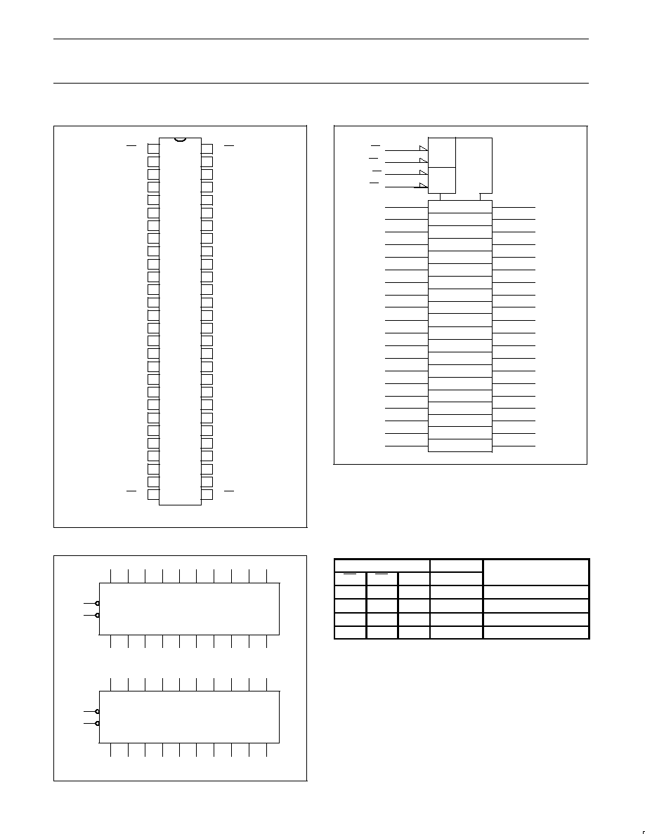
56-Pin Plastic TSSOP Type II
≠40
∞
C to +85
∞
C
74ALVCH162827DGG
ACH162827DGG
SOT364-1
PIN DESCRIPTION
PIN NUMBER
SYMBOL
FUNCTION
55, 54, 52, 51, 49, 48, 47, 45, 44, 43,
42, 41, 40, 38, 37, 36, 34, 33, 31, 30
1A0 - 1A9
2A0 - 2A9
Data inputs
2, 3, 5, 6, 8, 9, 10, 12, 13, 14,
15, 16, 17, 19, 20, 21, 23, 24, 26, 27
1Y0 - 1Y9
2Y0 - 2Y9
Data outputs
1, 56,
28, 29
1OE1 1OE2,
2OE1, 2OE2
Output enable inputs (active-LOW)
4, 11, 18, 25, 32, 39, 46, 53
GND
Ground (0V)
7, 22, 35, 50
V
CC
Positive supply voltage

Philips Semiconductors
Product specification
74ALVCH162827
20-bit buffer/line driver, non-inverting, with 30
termination resistors (3-State)
1998 Sep 29
4
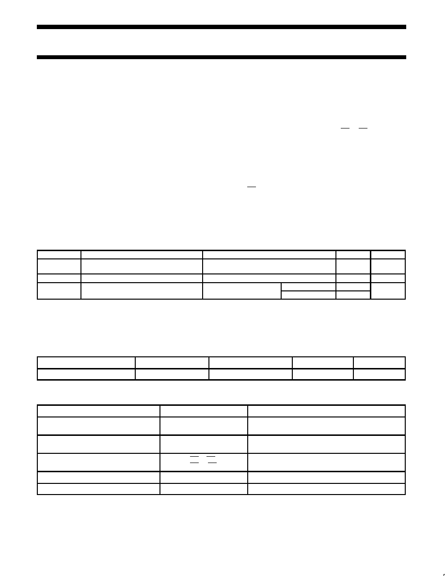
LOGIC DIAGRAM
nA0
nY0
nOE1
nA1
nY1
nA2
nY2
nA3
nY3
nA4
nY4
nA5
nY5
nA6
nY6
nA7
nY7
nA8
nY8
nA9
nY9
nOE2
SH00013
RECOMMENDED OPERATING CONDITIONS
SYMBOL
PARAMETER
CONDITIONS
MIN
MAX
UNIT
V
CC
DC supply voltage 2.5V range (for max. speed
performance @ 30 pF output load)
2.3
2.7
V
V
CC
DC supply voltage 3.3V range (for max. speed
performance @ 50 pF output load)
3.0
3.6
V
V
I
DC Input voltage range
0
V
CC
V
V
O
DC output voltage range
0
V
CC
V
T
amb
Operating free-air temperature range
≠40
+85
∞
C
t
r
, t
f
Input rise and fall times
V
CC
= 2.3 to 3.0V
V
CC
= 3.0 to 3.6V
0
0
20
10
ns/V
ABSOLUTE MAXIMUM RATINGS
In accordance with the Absolute Maximum Rating System (IEC 134)
Voltages are referenced to GND (ground = 0V)
SYMBOL
PARAMETER
CONDITIONS
RATING
UNIT
V
CC
DC supply voltage
≠0.5 to +4.6
V
I
IK
DC input diode current
V
I
t
0
≠50
mA
V
I
DC input voltage
Note 1
≠0.5 to +4.6
V
I
OK
DC output diode current
V
O
u
V
CC
or V
O
t
0
"
50
mA
V
O
DC output voltage
Note 1
≠0.5 to V
CC
+0.5
V
I
O
DC output source or sink current
V
O
= 0 to V
CC
"
50
mA
I
GND
, I
CC
DC V
CC
or GND current
"
100
mA
T
stg
Storage temperature range
≠65 to +150
∞
C
P
TOT
Power dissipation per package
≠plastic thin-medium-shrink (TSSOP)
For temperature range: ≠40 to +125
∞
C
above +55
∞
C derate linearly with 8 mW/K
600
mW
NOTE:
1. The input and output voltage ratings may be exceeded if the input and output current ratings are observed.
Philips Semiconductors
Product specification
74ALVCH162827
20-bit buffer/line driver, non-inverting, with 30
termination resistors (3-State)
1998 Sep 29
5
DC ELECTRICAL CHARACTERISTICS
Over recommended operating conditions. Voltage are referenced to GND (ground = 0 V).
LIMITS
SYMBOL
PARAMETER
TEST CONDITIONS
Temp = -40
∞
C to +85
∞
C
UNIT
MIN
TYP
1
MAX
V
HIGH level Input voltage
V
CC
= 2.3 to 2.7V
1.7
1.2
V
V
IH
HIGH level Input voltage
V
CC
= 2.7 to 3.6V
2.0
1.5
V
V
LOW level Input voltage
V
CC
= 2.3 to 2.7V
1.2
0.7
V
V
IL
LOW level Input voltage
V
CC
= 2.7 to 3.6V
1.5
0.8
V
V
CC
= 2 3 to 3 6V; V = V
or V ; I
O
= 100
µ
A
V
CC
0 2
V
CC
V
CC
= 2.3 to 3.6V; V
I
= V
IH
or V
IL
; I
O
= ≠100
µ
A
V
CC
*
0.2
V
CC
V
CC
= 2.3V; V
I
= V
IH
or V
IL
; I
O
= ≠4mA
V
CC
*
0.4
V
CC
*
0.11
V
CC
= 2.3V; V
I
= V
IH
or V
IL
; I
O
= ≠6mA
V
CC
*
0.6
V
CC
*
0.17
V
OH
HIGH level output voltage
V
CC
= 2.7V; V
I
= V
IH
or V
IL
; I
O
= ≠4mA
V
CC
*
0.5
V
CC
*
0.09
V
V
CC
= 2.7V; V
I
= V
IH
or V
IL
; I
O
= ≠8mA
V
CC
*
0.7
V
CC
*
0.19
V
CC
= 3.0V; V
I
= V
IH
or V
IL
; I
O
= ≠6mA
V
CC
*
0.6
V
CC
*
0.13
V
CC
= 3.0V; V
I
= V
IH
or V
IL;
I
O
= ≠12mA
V
CC
*
1.0
V
CC
*
0.27
V
= 2 3 to 3 6V; V = V
or V ; I = 100
µ
A
GND
0 20
V
CC
= 2.3 to 3.6V; V
I
= V
IH
or V
IL
; I
O
= 100
µ
A
GND
0.20
V
CC
= 2.3V; V
I
= V
IH
or V
IL
; I
O
= 4mA
0.07
0.40
V
CC
= 2.3V; V
I
= V
IH
or V
IL
; I
O
= 6mA
0.11
0.55
V
OL
LOW level output voltage
V
CC
= 2.7V; V
I
= V
IH
or V
IL
; I
O
= 4mA
0.06
0.40
V
V
CC
= 2.7V; V
I
= V
IH
or V
IL
; I
O
= 8mA
0.13
0.60
V
CC
= 3.0V; V
I
= V
IH
or V
IL;
I
O
= 6mA
0.09
0.55
V
CC
= 3.0V; V
I
= V
IH
or V
IL;
I
O
= 12mA
0.19
0.80
V
CC
= 2 3 to 3 6V;
I
I
Input leakage current
V
CC
= 2.3 to 3.6V;
V
V
or GND
0.1
5
µ
A
I
g
V
I
= V
CC
or GND
µ
I
OZ
3-State output OFF-state current
V
CC
= 2.3 to 3.6V; V
I
= V
IH
or V
IL
;
V
O
= V
CC
or GND
0.1
10
µ
A
I
CC
Quiescent supply current
V
CC
= 2.3 to 3.6V; V
I
= V
CC
or GND; I
O
= 0
0.2
40
µ
A
I
CC
Additional quiescent supply current
V
CC
= 2.3V to 3.6V; V
I
= V
CC
≠ 0.6V; I
O
= 0
150
750
µ
A
I
BHL
Bus hold LOW sustaining current
V
CC
= 2.3V; V
I
= 0.7V
2
45
≠
µ
A
I
Bus hold HIGH sustaining current
V
CC
= 2.3V; V
I
= 1.7V
2
≠45
µ
A
I
BHH
Bus hold HIGH sustaining current
V
CC
= 3.0V; V
I
= 2.0V
2
≠75
≠175
µ
A
I
BHLO
Bus hold LOW overdrive current
V
CC
= 3.6V
2
500
µ
A
I
BHHO
Bus hold HIGH overdrive current
V
CC
= 3.6V
2
≠500
µ
A
NOTES:
1. All typical values are at T
amb
= 25
∞
C.
2. Valid for data inputs of bus hold parts.