1999 Nov 23
2
Philips Semiconductors
Product specification
16-bit D-type registered transceiver; 3-state
74ALVCH16543
FEATURES
∑
In accordance with JEDEC standard no 8-1A
∑
CMOS low power consumption
∑
Direct interface with TTL levels
∑
MULTIBYTE
TM
flow-through pin-out architecture
∑
16-bit transceiver with D-type latch
∑
Combines 16245 and 16373 type functions in one chip
∑
Back-to-back registers for storage
∑
Output drive capability 50
transmission lines at 85
∞
C
∑
Separate controls for data flow in each direction
∑
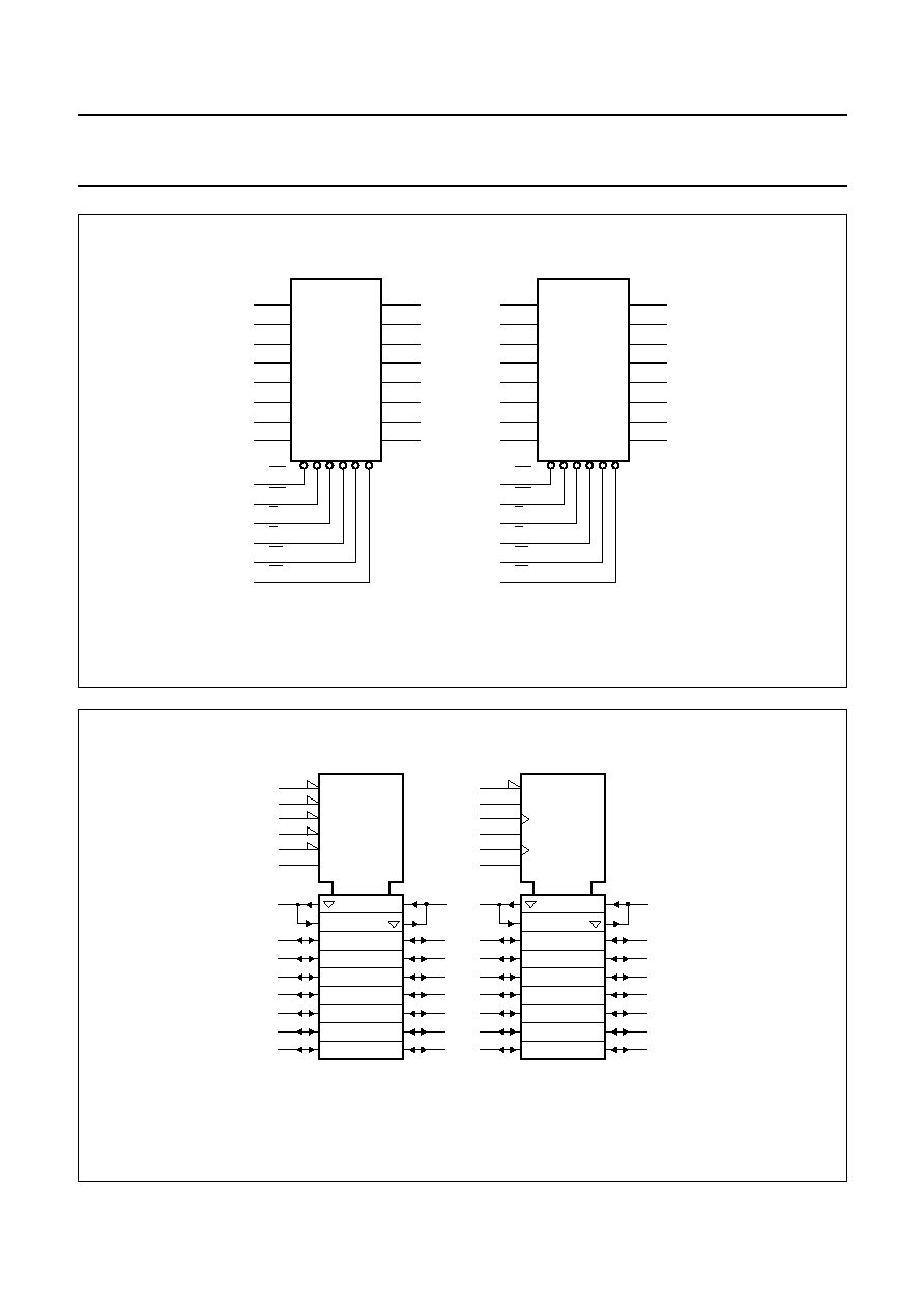
All data inputs have bus hold
∑
3-state non-inverting outputs for bus oriented
applications
∑
Current drive
±
24 mA at 3.0 V.
DESCRIPTION
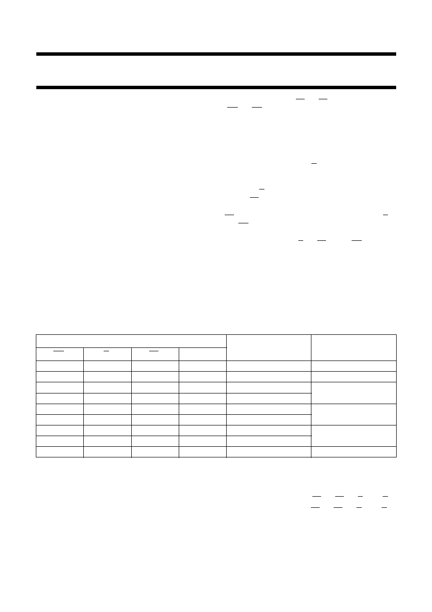
The 74ALVCH16543 is a dual octal registered transceiver.
Each section contains two sets of D-type latches for
temporary storage of the data flow in either direction.
Separate latch enable (nLE
AB
, nLE
BA
) and output enable
(nOE
AB
, nOE
BA
) inputs are provided for each register to
permit independent control in either direction of the data
flow.
The `16543' contains two sections each consisting of two
sets of eight D-type latches with separate inputs and
controls for each set. For data flow from A to B, for
example, the A-to-B enable (nE
AB
, where n equals 1 or 2)
inputs must be LOW in order to enter data from nA
0
to nA
7
,
or take data from nB
0
to nB
7
, as indicated in the function
table. With nE
AB
LOW, a LOW signal on the A-to-B latch
enable (nLE
AB
) input makes the A-to-B latches
transparent; a subsequent LOW-to-HIGH transition of the
nLE
AB
signal stores the A data into the latches. With nE
AB
and nOE
AB
both LOW, the 3-state B output buffers are
active and display the data present at the output of the
A latches. Similarly, the nE
BA
, nLE
BA
and nOE
BA
signals
control the data flow from B-to-A.
Active bus hold circuitry is provided to hold unused or
floating data inputs at a valid logic level.
FUNCTION TABLE
See note 1.
Note
1. XX = AB for A-to-B direction, BA for B-to-A direction;
H = HIGH voltage level; L = LOW voltage level;
h = HIGH state must be present one set-up time before the LOW-to-HIGH transition of nLE
AB
, nLE
BA
, nE
AB
or nE
BA
;
l = LOW state must be present one set-up time before the LOW-to-HIGH transition of nLE
AB
, nLE
BA
, nE
AB
or nE
BA
;
X = don't care; NC = no change;
= LOW-to-HIGH level transition;
Z = high-impedance OFF-state.
INPUTS
OUTPUTS
STATUS
nOE
XX
nE
XX
nLE
XX
nB
n
, nA
n
H
X
X
X
Z
disabled
X
H
X
X
Z
disabled
L
L
h
Z
disabled and latch
L
L
l
Z
L
L
h
H
latch and display
L
L
l
L
L
L
L
H
H
transparent
L
L
L
L
L
L
L
H
X
NC
hold
1999 Nov 23
3
Philips Semiconductors
Product specification
16-bit D-type registered transceiver; 3-state
74ALVCH16543
QUICK REFERENCE DATA
Ground = 0; T
amb
= 25
∞
C; t
r
= t
f
= 2.5 ns
Notes
1. C
PD
is used to determine the dynamic power dissipation (P
D
in
µ
W).
P
D
= C
PD
◊
V
CC
2
◊
f
i
+
(C
L
◊
V
CC
2
◊
f
o
) where:
f
i
= input frequency in MHz;
C
L
= output load capacitance in pF;
f
o
= output frequency in MHz;
V
CC
= supply voltage in Volts;
(C
L
◊
V
CC
2
◊
f
o
) = sum of outputs.
2. The condition is V
I
= GND to V
CC
.
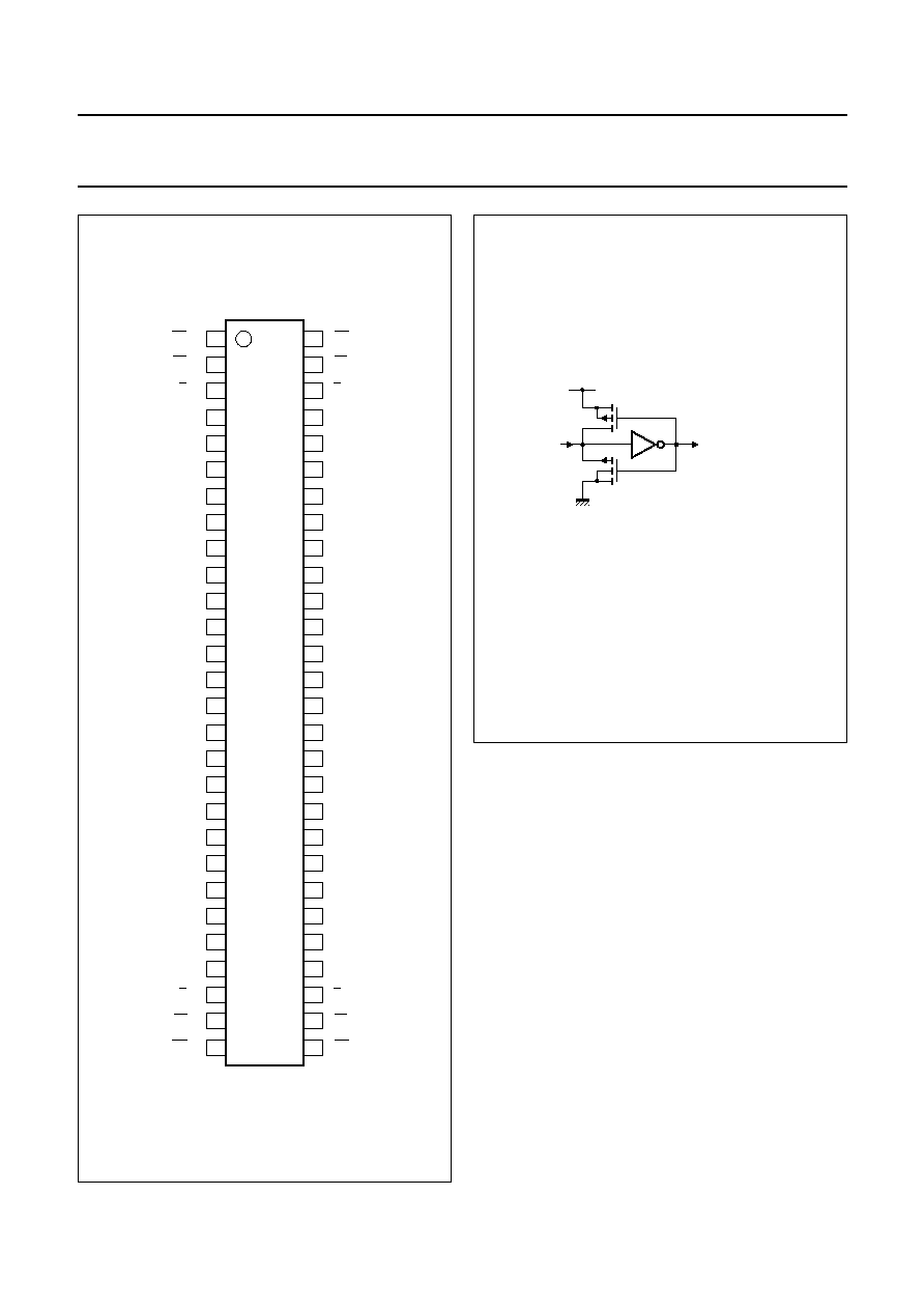
ORDERING INFORMATION
PINNING
SYMBOL
PARAMETER
CONDITIONS
TYPICAL
UNIT
t
PHL
/t
PLH
propagation delay nA
n
, nB
n
to nB
n
, nA
n
C
L
= 50 pF;
V
CC
= 3.3 V
3.8
ns
C
I
input capacitance
4.0
pF
C
PD
power dissipation capacitance per latch
notes 1 and 2
outputs enabled
44
pF
outputs disabled
14
pF
OUTSIDE NORTH
AMERICA
NORTH
AMERICA
PACKAGE
TEMPERATURE
RANGE
PINS
PACKAGE
MATERIAL
CODE
74ALVCH16543DGG
ACH16543 DGG
-
40 to +85
∞
C
56
TSSOP
plastic
SOT364-1
PIN
SYMBOL
DESCRIPTION
1 and 28
1OE
AB
, 2OE
AB
output enable A-to-B for register 1 or 2
2 and 27
1LE
AB
, 2LE
AB
latch enable A-to-B for register 1 or 2
3 and 26
1E
AB
, 2E
AB
A-to-B enable for register 1 or 2
4, 11, 18, 25, 32, 39, 46 and 53
GND
ground (0 V)
5, 6, 8, 9, 10, 12, 13 and 14
1A
0
to 1A
7
data inputs/outputs
7, 22, 35 and 50
V
CC
DC supply voltage
15, 16, 17, 19, 20, 21, 23 and 24
2A
0
to 2A
7
data inputs/outputs
29 and 56
2OE
BA
, 1OE
BA
output enable B-to-A for register 1 or 2
30 and 55
2LE
BA
, 1LE
AB
latch enable B-to-A for register 1 or 2
31 and 54
2E
BA
, 1E
BA
B-to-A enable for register 1 or 2
33, 34, 36, 37, 38, 40, 41 and 42
2B
7
to 2B
0
data inputs/outputs
43, 44, 45, 47, 48, 49, 51 and 52
1B
7
to 1B
0
data inputs/outputs