Philips Semiconductors
Product specification
74ALVCH16827
20-bit buffer/line driver, non-inverting (3-State)
2
1998 Jul 27
853-2096 19785
FEATURES
∑
Wide supply voltage range of 1.2V to 3.6V
∑
Complies with JEDEC standard no. 8-1A
∑
Wide supply voltage range of 1.2V to 3.6V
∑
CMOS low power consumption
∑
Direct interface with TTL levels
∑
Universal bus transceiver with D-type latches and D-type flip-flops
capable of operating in transparent, latched, clocked or
clocked-enabled mode.
∑
MULTIBYTE
TM
flow-through standard pin-out architecture
∑
Low inductance multiple V
CC
and GND pins for minimum noise
and ground bounce
∑
Current drive
±
24 mA at 3.0 V
∑
All inputs have bus hold circuitry
∑
Output drive capability 50
transmission lines @ 85
∞
C
∑
3-State non-inverting outputs for bus oriented applications
DESCRIPTION
The 74ALVCH16827 is a 20-bit non-inverting buffer/driver with
3-State outputs for bus oriented applications.
The 74ALVCH16827 consists of two 10-bit sections with separate
output enable signals. For either 10-bit buffer section, the two output
enable (1OE1 and 1OE2 or 2OE1 and 2OE2) inputs must both be
active. If either output enable input is high, the outputs of that 10-bit
buffer section are in high impedance state.
The 74ALVCH16827 has active bus hold circuitry which is provided
to hold unused or floating data inputs at a valid logic level. This
feature eliminates the need for external pull-up or pull-down
resistors.
QUICK REFERENCE DATA
GND = 0V; T
amb
= 25
∞
C; t
r
= t
f
= 2.5ns
SYMBOL
PARAMETER
CONDITIONS
TYPICAL
UNIT
t
PHL
/t
PLH
Propagation delay
CP to Qn
V
CC
= 2.5V, C
L
= 30pF
V
CC
= 3.3V, C
L
= 50pF
2.0
2.0
ns
C
I
Input capacitance
5
pF
C
PD
Power dissipation capacitance per latch
V
I
= GND to V
CC
1
Output enabled
20
pF
C
PD
Power dissi ation ca acitance er latch
V
I
= GND to V
CC
1
Output disabled
3
F
NOTES:
1.
C
PD
is used to determine the dynamic power dissipation (P
D
in
m
W):
P
D
= C
PD
◊
V
CC
2
◊
f
i
+
S
(C
L
◊
V
CC
2
◊
f
o
) where:
f
i
= input frequency in MHz; C
L
= output load capacity in pF;
f
o
= output frequency in MHz; V
CC
= supply voltage in V;
S
(C
L
◊
V
CC
2
◊
f
o
) = sum of outputs.
ORDERING INFORMATION
PACKAGES
TEMPERATURE RANGE
OUTSIDE NORTH AMERICA
NORTH AMERICA
DWG NUMBER
56-Pin Plastic TSSOP Type II
≠40
∞
C to +85
∞
C
74ALVCH16827 DGG
ACH16827 DGG
SOT364-1
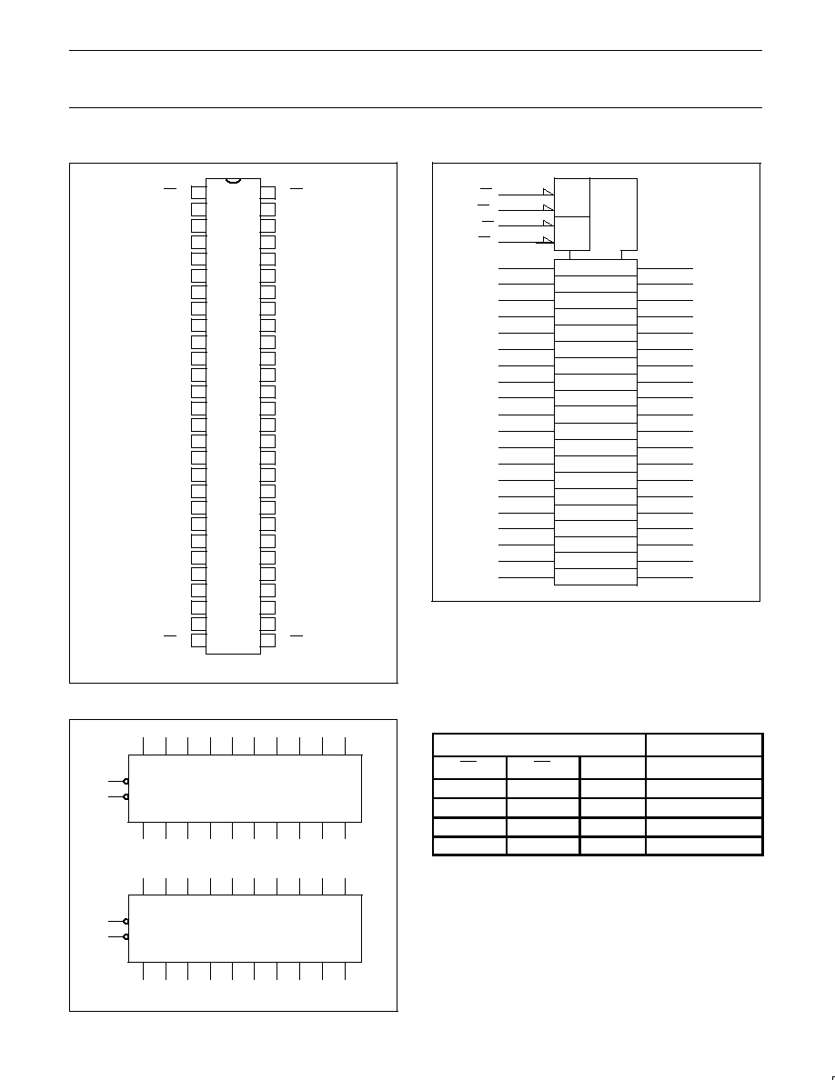
PIN DESCRIPTION
PIN NUMBER
SYMBOL
FUNCTION
55, 54, 52, 51, 49, 48, 47, 45, 44, 43,
42, 41, 40, 38, 37, 36, 34, 33, 31, 30
1A0 - 1A9
2A0 - 2A9
Data inputs
2, 3, 5, 6, 8, 9, 10, 12, 13, 14,
15, 16, 17, 19, 20, 21, 23, 24, 26, 27
1Y0 - 1Y9
2Y0 - 2Y9
Data outputs
1, 56,
28, 29
1OE0, 1OE1
2OE0, 2OE1
Output enable inputs (active-Low)
4, 11, 18, 25, 32, 39, 46, 53
GND
Ground (0V)
7, 22, 35, 50
V
CC
Positive supply voltage
Philips Semiconductors
Product specification
74ALVCH16827
20-bit buffer/line driver, non-inverting (3-State)
1998 Jul 27
4
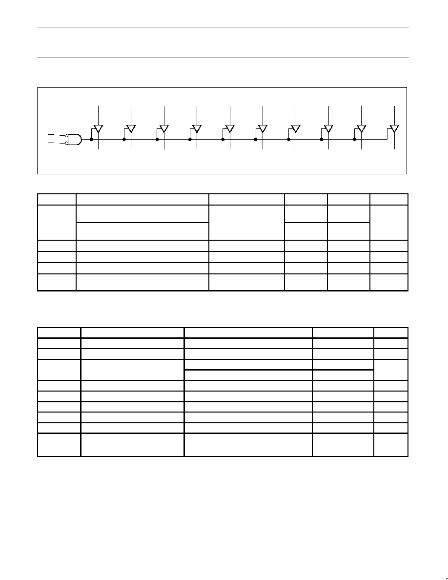
LOGIC DIAGRAM
nA0
nY0
nOE1
nA1
nY1
nA2
nY2
nA3
nY3
nA4
nY4
nA5
nY5
nA6
nY6
nA7
nY7
nA8
nY8
nA9
nY9
nOE2
SH00013
RECOMMENDED OPERATING CONDITIONS
SYMBOL
PARAMETER
CONDITIONS
MIN
MAX
UNIT
V
CC
DC supply voltage 2.5V range (for max. speed
performance @ 30 pF output load)
2.3
2.7
V
V
CC
DC supply voltage 3.3V range (for max. speed
performance @ 50 pF output load)
3.0
3.6
V
V
I
DC Input voltage range
0
V
CC
V
V
O
DC output voltage range
0
V
CC
V
T
amb
Operating free-air temperature range
≠40
+85
∞
C
t
r
, t
f
Input rise and fall times
V
CC
= 2.3 to 3.0V
V
CC
= 3.0 to 3.6V
0
0
20
10
ns/V
ABSOLUTE MAXIMUM RATINGS
1
In accordance with the Absolute Maximum Rating System (IEC 134)
Voltages are referenced to GND (ground = 0V)
SYMBOL
PARAMETER
CONDITIONS
RATING
UNIT
V
CC
DC supply voltage
≠0.5 to +4.6
V
I
IK
DC input diode current
V
I
t
0
≠50
mA
V
I
DC input voltage
For control pins
2
≠0.5 to +4.6
V
V
I
DC in ut voltage
For data inputs
2
≠0.5 to V
CC
+0.5
V
I
OK
DC output diode current
V
O
u
V
CC
or V
O
t
0
"
50
mA
V
O
DC output voltage
Note 2
≠0.5 to V
CC
+0.5
V
I
O
DC output source or sink current
V
O
= 0 to V
CC
"
50
mA
I
GND
, I
CC
DC V
CC
or GND current
"
100
mA
T
stg
Storage temperature range
≠65 to +150
∞
C
P
TOT
Power dissipation per package
≠plastic medium-shrink (SSOP)
≠plastic thin-medium-shrink (TSSOP)
For temperature range: ≠40 to +125
∞
C
above +55
∞
C derate linearly with 11.3 mW/K
above +55
∞
C derate linearly with 8 mW/K
850
600
mW
NOTE:
1. Stresses beyond those listed may cause permanent damage to the device. These are stress ratings only and functional operation of the
device at these or any other conditions beyond those indicated under "recommended operating conditions" is not implied. Exposure to
absolute-maximum-rated conditions for extended periods may affect device reliability.
2. The input and output voltage ratings may be exceeded if the input and output current ratings are observed.
Philips Semiconductors
Product specification
74ALVCH16827
20-bit buffer/line driver, non-inverting (3-State)
1998 Jul 27
5
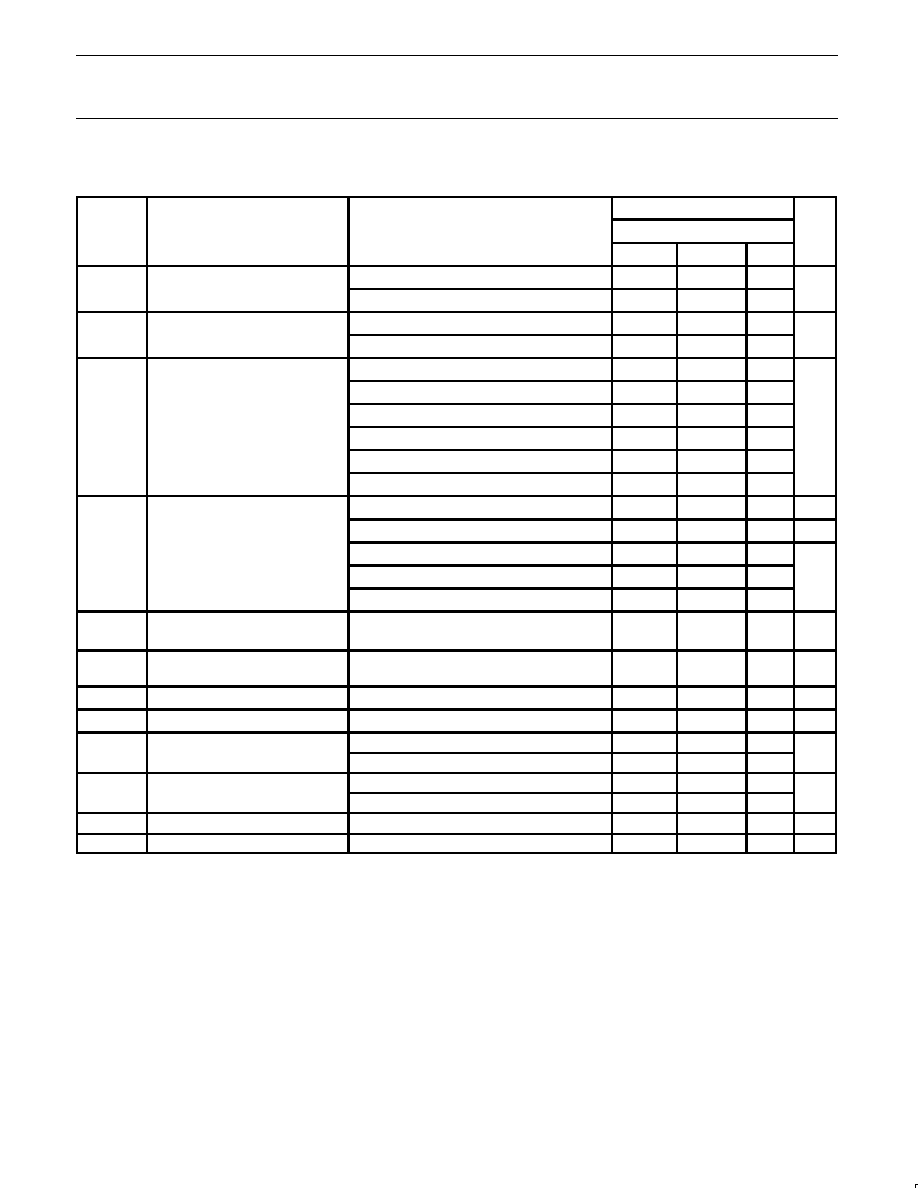
DC ELECTRICAL CHARACTERISTICS
Over recommended operating conditions. Voltage are referenced to GND (ground = 0 V).
LIMITS
SYMBOL
PARAMETER
TEST CONDITIONS
Temp = -40
∞
C to +85
∞
C
UNIT
MIN
TYP
1
MAX
V
HIGH level Input voltage
V
CC
= 2.3 to 2.7V
1.7
1.2
V
V
IH
HIGH level Input voltage
V
CC
= 2.7 to 3.6V
2.0
1.5
V
V
LOW level Input voltage
V
CC
= 2.3 to 2.7V
1.2
0.7
V
V
IL
LOW level Input voltage
V
CC
= 2.7 to 3.6V
1.5
0.8
V
V
CC
= 2 3 to 3 6V; V = V
or V ; I
O
= 100
µ
A
V
CC
0 2
V
CC
V
CC
= 2.3 to 3.6V; V
I
= V
IH
or V
IL
; I
O
= ≠100
µ
A
V
CC
*
0.2
V
CC
V
CC
= 2.3V; V
I
= V
IH
or V
IL
; I
O
= ≠6mA
V
CC
*
0.3
V
CC
*
0.08
V
O
HIGH level output voltage
V
CC
= 2.3V; V
I
= V
IH
or V
IL
; I
O
= ≠12mA
V
CC
*
0.6
V
CC
*
0.26
V
V
OH
HIGH level output voltage
V
CC
= 2.7V; V
I
= V
IH
or V
IL
; I
O
= ≠12mA
V
CC
*
0.5
V
CC
*
0.14
V
V
CC
= 3.0V; V
I
= V
IH
or V
IL
; I
O
= ≠12mA
V
CC
*
0.6
V
CC
*
0.09
V
CC
= 3.0V; V
I
= V
IH
or V
IL;
I
O
= ≠24mA
V
CC
*
1.0
V
CC
*
0.28
V
= 2 3 to 3 6V; V = V
or V ; I = 100
µ
A
GND
0 20
V
V
CC
= 2.3 to 3.6V; V
I
= V
IH
or V
IL
; I
O
= 100
µ
A
GND
0.20
V
V
CC
= 2.3V; V
I
= V
IH
or V
IL
; I
O
= 6mA
0.07
0.40
V
V
OL
LOW level output voltage
V
CC
= 2.3V; V
I
= V
IH
or V
IL
; I
O
= 12mA
0.15
0.70
V
CC
= 2.7V; V
I
= V
IH
or V
IL
; I
O
= 12mA
0.14
0.40
V
V
CC
= 3.0V; V
I
= V
IH
or V
IL;
I
O
= 24mA
0.27
0.55
V
CC
= 2 3 to 3 6V;
I
I
Input leakage current
V
CC
= 2.3 to 3.6V;
V
V
or GND
0.1
5
µ
A
I
g
V
I
= V
CC
or GND
µ
I
OZ
3-State output OFF-state current
V
CC
= 2.3 to 3.6V; V
I
= V
IH
or V
IL
;
V
O
= V
CC
or GND
0.1
10
µ
A
I
CC
Quiescent supply current
V
CC
= 2.3 to 3.6V; V
I
= V
CC
or GND; I
O
= 0
0.2
40
µ
A
I
CC
Additional quiescent supply current
V
CC
= 2.3V to 3.6V; V
I
= V
CC
≠ 0.6V; I
O
= 0
150
750
µ
A
I
BHL
2
Bus hold LOW sustaining current
V
CC
= 2.3V; V
I
= 0.7V
45
≠
µ
A
I
BHL
2
Bus hold LOW sustaining current
V
CC
= 3.0V; V
I
= 0.8V
75
150
µ
A
I
BHH
2
Bus hold HIGH sustaining current
V
CC
= 2.3V; V
I
= 1.7V
≠45
µ
A
I
BHH
2
Bus hold HIGH sustaining current
V
CC
= 3.0V; V
I
= 2.0V
≠75
≠175
µ
A
I
BHLO
2
Bus hold LOW overdrive current
V
CC
= 3.6V
500
µ
A
I
BHHO
2
Bus hold HIGH overdrive current
V
CC
= 3.6V
≠500
µ
A
NOTES:
1. All typical values are at T
amb
= 25
∞
C.
2. Valid for data inputs of bus hold parts.