Philips
Semiconductors
74ALVCH16841
20-bit bus interface D-type latch (3-State)
Product specification
IC24 Data Handbook
1998 Jul 27
INTEGRATED CIRCUITS
Philips Semiconductors
Product specification
74ALVCH16841
20-bit bus interface D-type latch (3-State)
2
1998 Jul 27
853-2093 19785
FEATURES
∑
Wide supply voltage range of 1.2V to 3.6V
∑
Complies with JEDEC standard no. 8-1A
∑
Wide supply voltage range of 1.2V to 3.6V
∑
CMOS low power consumption
∑
Direct interface with TTL levels
∑
MULTIBYTE
TM
flow-through standard pin-out architecture
∑
Low inductance multiple V
CC
and GND pins for minimum noise
and ground bounce
∑
Current drive
±
24 mA at 3.0 V
∑
All inputs have bus hold circuitry
∑
Output drive capability 50
transmission lines @ 85
∞
C
∑
3-State non-inverting outputs for bus oriented applications
DESCRIPTION
The 74ALVCH16841 has two 10-bit D-type latch featuring separate
D-type inputs for each latch and 3-State outputs for bus oriented
applications. The two sections of each register are controlled
independently by the latch enable (nLE) and output enable (nOE)
control gates.
When nOE is LOW, the data in the registers appears at the outputs.
When nOE is High the outputs are in High-impedance OFF state.
Operation of the nOE input does not affect the state of the flip-flops.
The 74ALVCH16841 has active bus hold circuitry which is provided
to hold unused or floating data inputs at a valid logic level. This
feature eliminates the need for external pull-up or pull-down
resistors.
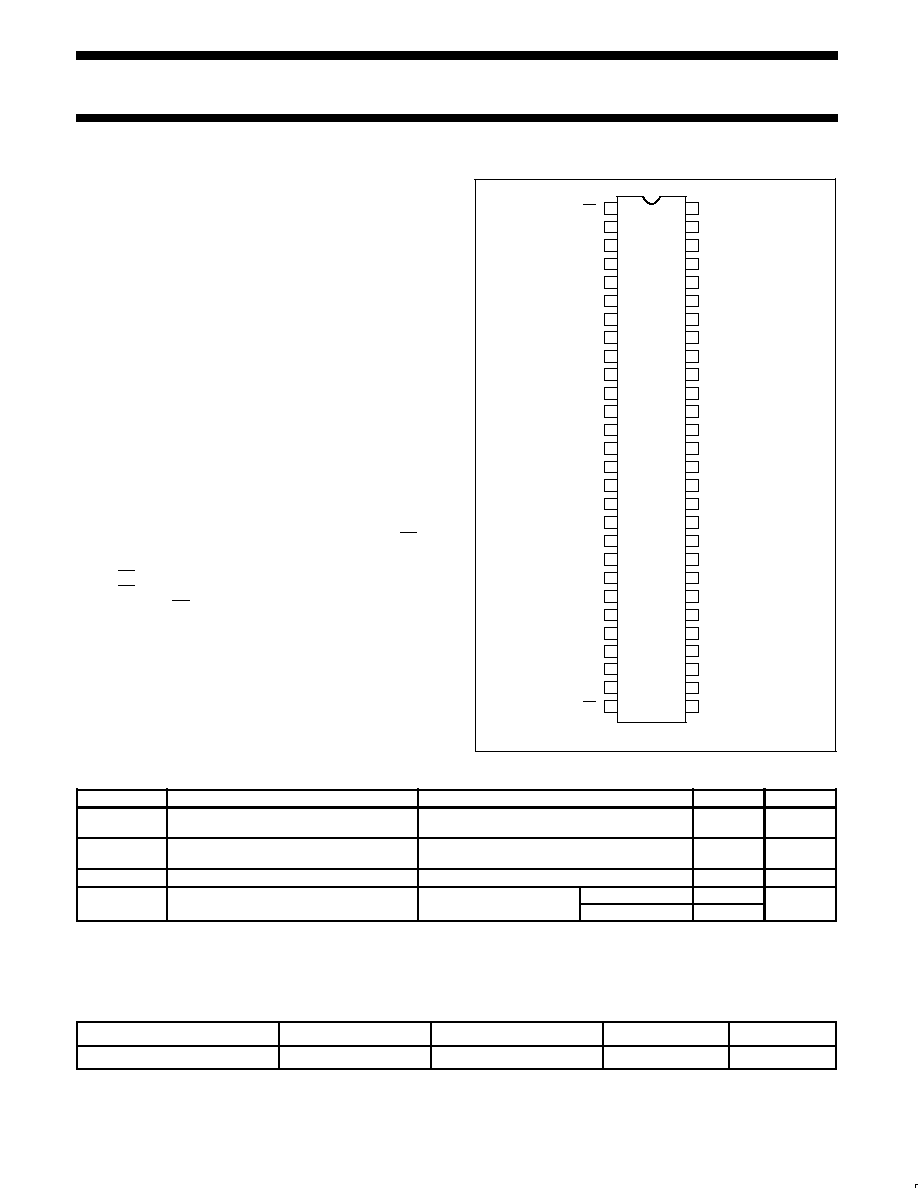
PIN CONFIGURATION
1
2
3
4
5
6
7
8
9
10
11
12
13
14
15
16
17
18
19
20
21
22
23
24
48
47
46
45
44
43
42
41
40
39
38
37
36
35
34
33
32
31
30
29
1OE
1Q0
1Q1
GND
1Q2
1Q3
1Q4
1Q5
GND
1Q6
1Q7
1Q8
2Q2
1Q9
VCC
2Q3
VCC
2Q1
2Q4
2Q8
2OE
2Q7
1LE
1D0
1D1
GND
1D2
1D3
1D4
1D5
2D0
1D6
1D7
2D1
2D2
GND
2D4
VCC
2D5
VCC
2D3
2D6
GND
2D8
2LE
2D7
SA00076
2Q0
GND
2Q5
28
27
26
25
49
50
51
52
53
54
55
56
2D9
1D9
1D8
GND
2Q9
GND
2Q6
QUICK REFERENCE DATA
GND = 0V; T
amb
= 25
∞
C; t
r
= t
f
2.5ns
SYMBOL
PARAMETER
CONDITIONS
TYPICAL
UNIT
t
PHL
/t
PLH
Propagation delay
nD
n
to nQ
n
V
CC
= 2.5V, C
L
= 30pF
V
CC
= 3.3V, C
L
= 50pF
2.5
2.4
ns
t
PHL
/t
PLH
Propagation delay
nLE to nQ
n
V
CC
= 2.5V, C
L
= 30pF
V
CC
= 3.3V, C
L
= 50pF
2.5
2.4
ns
C
I
Input capacitance
5.0
pF
C
PD
Power dissipation capacitance per buffer
V
I
= GND to V
CC
1
Outputs enabled
19
pF
C
PD
Power dissi ation ca acitance er buffer
V
I
= GND to V
CC
1
Outputs disabled
3
F
NOTES:
1. C
PD
is used to determine the dynamic power dissipation (P
D
in
µ
W):
P
D
= C
PD
◊
V
CC
2
◊
f
i
+
S
(C
L
◊
V
CC
2
◊
f
o
) where: f
i
= input frequency in MHz; C
L
= output load capacitance in pF;
f
o
= output frequency in MHz; V
CC
= supply voltage in V;
S
(C
L
◊
V
CC
2
◊
f
o
) = sum of outputs.
ORDERING INFORMATION
PACKAGES
TEMPERATURE RANGE
OUTSIDE NORTH AMERICA
NORTH AMERICA
DWG NUMBER
56-Pin Plastic TSSOP Type II
≠40
∞
C to +85
∞
C
74ALVCH16841 DGG
ACH16841 DGG
SOT364-1
Philips Semiconductors
Product specification
74ALVCH16841
20-bit bus interface D-type latch (3-State)
1998 Jul 27
3
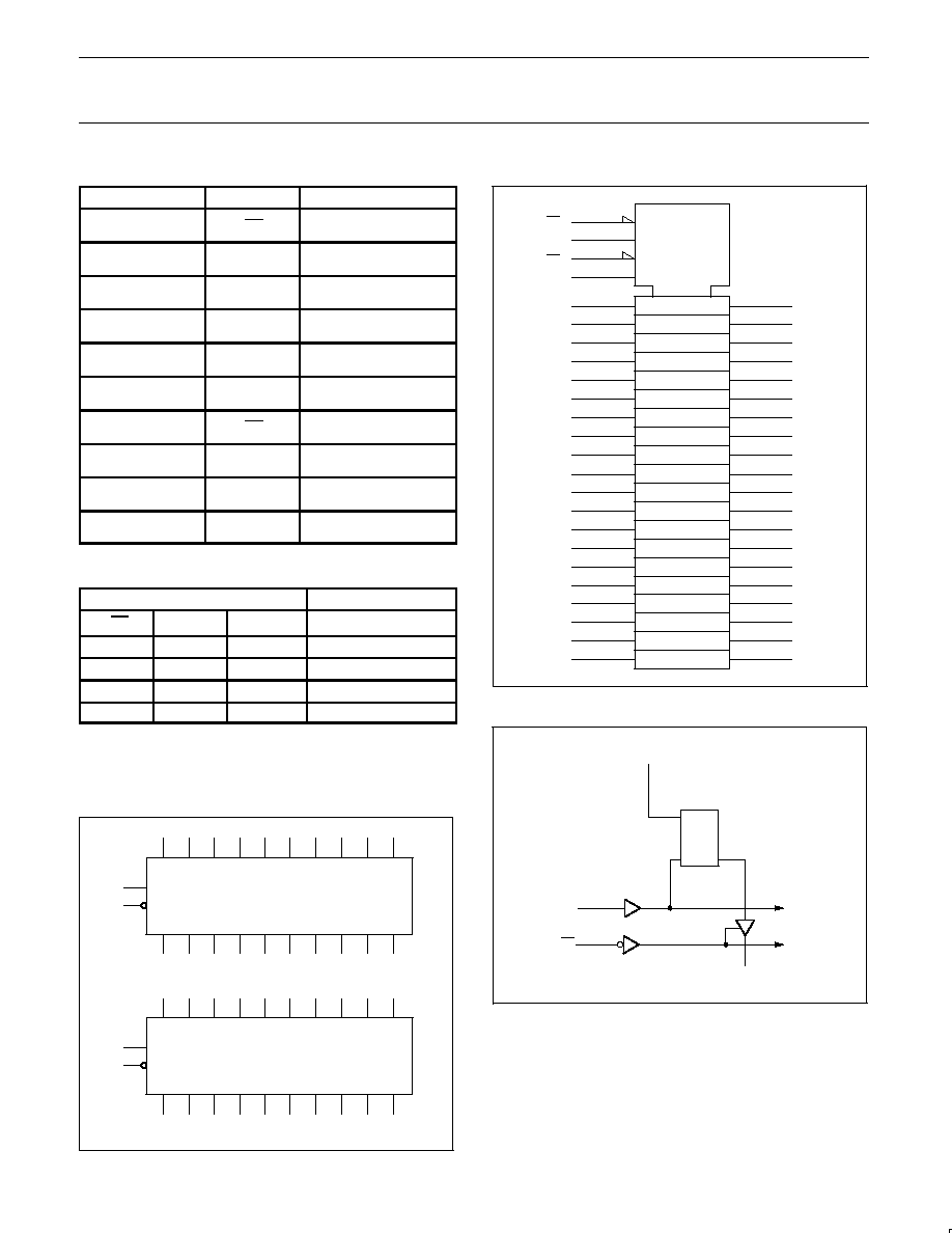
PIN DESCRIPTION
PIN NUMBER
SYMBOL
FUNCTION
1
1OE
Output enable inputs
(active-LOW)
56
1LE
Latch enable inputs
(active HIGH)
55, 54, 52, 51, 49,
48, 47, 45, 44, 43
1D0 ≠ 1D9
Data inputs
2, 3, 5, 6, 8, 9, 10,
12, 13, 14
1Q0 ≠ 1Q9
Data outputs
4, 11, 18, 25, 32,
39, 46, 53
GND
Ground (0V)
7, 22, 35, 50
V
CC
Positive supply
voltage
28
2OE
Output enable inputs
(active-LOW)
29
2LE
Latch enable inputs
(active HIGH)
42, 41, 40, 38, 37,
36, 34, 33, 31, 30
2D0 ≠ 2D9
Data inputs
15, 16, 17, 19, 20,
21, 23, 24, 26, 27
2Q0 ≠ 2Q9
Data outputs
FUNCTION TABLE
INPUTS
OUTPUT
nOE
LE
Dx
Q
L
H
L
L
L
H
H
H
L
L
X
Q
0
H
X
X
Z
H = High voltage level
L
= Low voltage level
X = Don't care
Z = High impedance "off" state
LOGIC SYMBOL
1D0 1D1 1D2 1D3 1D4 1D5 1D6
1D7
1Q0 1Q1 1Q2 1Q3 1Q4 1Q5 1Q6
1Q7
1D8
1D9
1Q8
1Q9
2D0 2D1 2D2 2D3 2D4 2D5 2D6
2D7
2Q0 2Q1 2Q2 2Q3 2Q4 2Q5 2Q6
2Q7
2D8
2D9
2Q8
2Q9
55
54
52
51
49
48
47
45
44
43
56
1
29
28
2
3
5
6
8
9
10
12
13
14
42
41
40
38
37
36
34
33
31
30
15
16
17
19
20
21
23
24
26
27
SH00023
1LE
1OE
2LE
2OE
LOGIC SYMBOL (IEEE/IEC)
1D0
1D1
1D2
1D3
1D4
1D5
1D6
1D7
1Q0
1Q1
1Q2
1Q3
1Q4
1Q5
1Q6
1Q7
1D8
1D9
1Q8
1Q9
2D0
2D1
2D2
2D3
2D4
2D5
2D6
2D7
2Q0
2Q1
2Q2
2Q3
2Q4
2Q5
2Q6
2Q7
2D8
2D9
2Q8
2Q9
EN4
2
EN2
4
1
56
28
29
55
54
52
51
49
48
47
45
44
43
42
41
40
38
37
36
34
33
31
30
2
3
5
6
8
9
10
12
13
14
15
16
17
19
20
21
23
24
26
27
1D
3D
C1
C3
1OE
1LE
2OE
2LE
SH00152
LOGIC DIAGRAM
nD
0
nQ
0
D
LE
nLE
nOE
SH00151
Philips Semiconductors
Product specification
74ALVCH16841
20-bit bus interface D-type latch (3-State)
1998 Jul 27
4
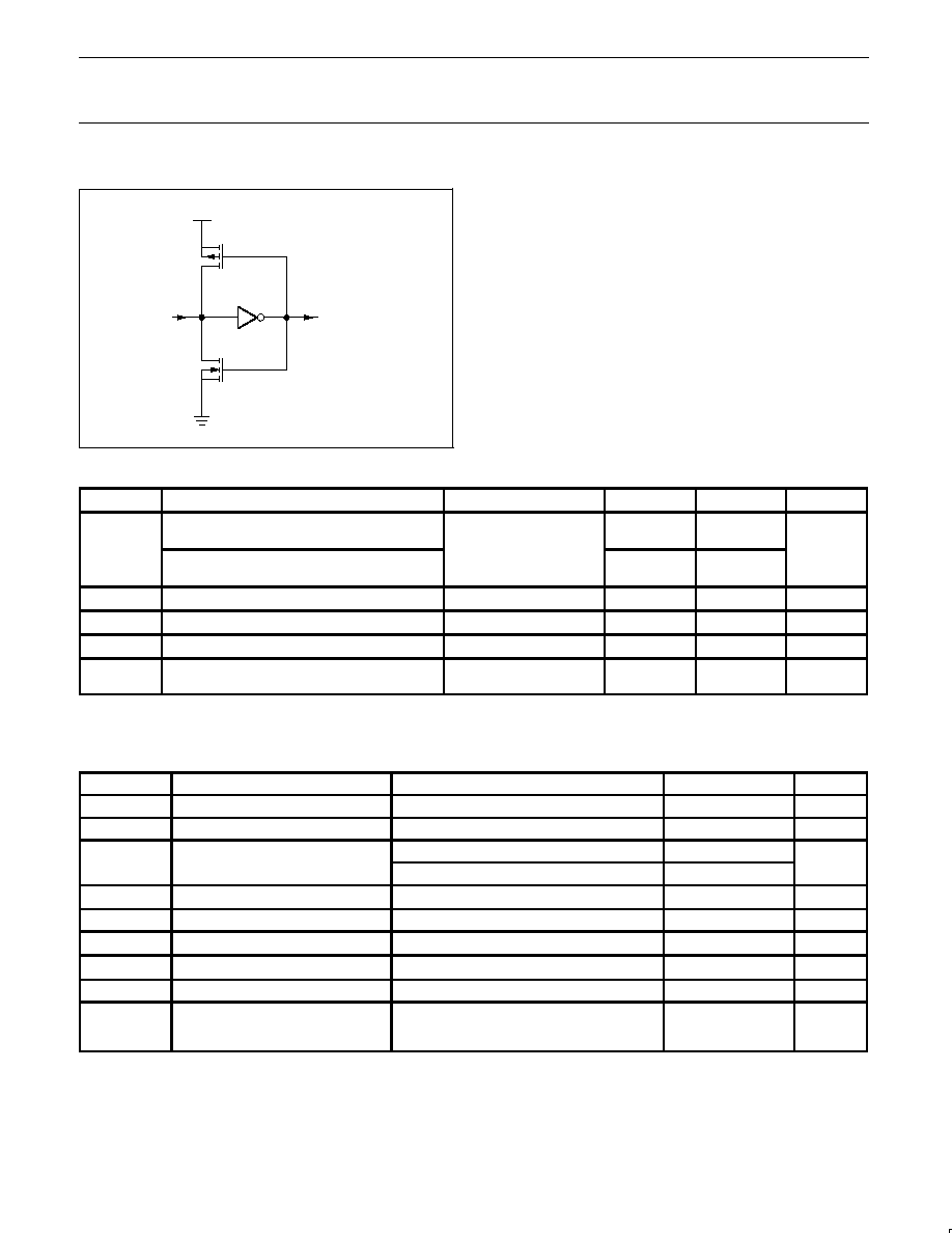
BUS HOLD CIRCUIT
To internal circuit
V
CC
Data Input
SW00044
RECOMMENDED OPERATING CONDITIONS
SYMBOL
PARAMETER
CONDITIONS
MIN
MAX
UNIT
V
CC
DC supply voltage 2.5V range (for max. speed
performance @ 30 pF output load)
2.3
2.7
V
V
CC
DC supply voltage 3.3V range (for max. speed
performance @ 50 pF output load)
3.0
3.6
V
V
I
DC Input voltage range
0
V
CC
V
V
O
DC output voltage range
0
V
CC
V
T
amb
Operating free-air temperature range
≠40
+85
∞
C
t
r
, t
f
Input rise and fall times
V
CC
= 2.3 to 3.0V
V
CC
= 3.0 to 3.6V
0
0
20
10
ns/V
ABSOLUTE MAXIMUM RATINGS
In accordance with the Absolute Maximum Rating System (IEC 134)
Voltages are referenced to GND (ground = 0V)
SYMBOL
PARAMETER
CONDITIONS
RATING
UNIT
V
CC
DC supply voltage
≠0.5 to +4.6
V
I
IK
DC input diode current
V
I
t
0
≠50
mA
V
I
DC input voltage
For control pins
1
≠0.5 to +4.6
V
V
I
DC in ut voltage
For data inputs
1
≠0.5 to V
CC
+0.5
V
I
OK
DC output diode current
V
O
u
V
CC
or V
O
t
0
"
50
mA
V
O
DC output voltage
Note 1
≠0.5 to V
CC
+0.5
V
I
O
DC output source or sink current
V
O
= 0 to V
CC
"
50
mA
I
GND
, I
CC
DC V
CC
or GND current
"
100
mA
T
stg
Storage temperature range
≠65 to +150
∞
C
P
TOT
Power dissipation per package
≠plastic medium-shrink (SSOP)
≠plastic thin-medium-shrink (TSSOP)
For temperature range: ≠40 to +125
∞
C
above +55
∞
C derate linearly with 11.3 mW/K
above +55
∞
C derate linearly with 8 mW/K
850
600
mW
NOTE:
1. The input and output voltage ratings may be exceeded if the input and output current ratings are observed.
Philips Semiconductors
Product specification
74ALVCH16841
20-bit bus interface D-type latch (3-State)
1998 Jul 27
5
DC ELECTRICAL CHARACTERISTICS
Over recommended operating conditions. Voltage are referenced to GND (ground = 0 V).
LIMITS
SYMBOL
PARAMETER
TEST CONDITIONS
Temp = -40
∞
C to +85
∞
C
UNIT
MIN
TYP
1
MAX
V
HIGH level Input voltage
V
CC
= 2.3 to 2.7V
1.7
1.2
V
V
IH
HIGH level Input voltage
V
CC
= 2.7 to 3.6V
2.0
1.5
V
V
LOW level Input voltage
V
CC
= 2.3 to 2.7V
1.2
0.7
V
V
IL
LOW level Input voltage
V
CC
= 2.7 to 3.6V
1.5
0.8
V
V
CC
= 2 3 to 3 6V; V = V
or V ; I
O
= 100
µ
A
V
CC
0 2
V
CC
V
CC
= 2.3 to 3.6V; V
I
= V
IH
or V
IL
; I
O
= ≠100
µ
A
V
CC
*
0.2
V
CC
V
CC
= 2.3V; V
I
= V
IH
or V
IL
; I
O
= ≠6mA
V
CC
*
0.3
V
CC
*
0.08
V
O
HIGH level output voltage
V
CC
= 2.3V; V
I
= V
IH
or V
IL
; I
O
= ≠12mA
V
CC
*
0.6
V
CC
*
0.26
V
V
OH
HIGH level output voltage
V
CC
= 2.7V; V
I
= V
IH
or V
IL
; I
O
= ≠12mA
V
CC
*
0.5
V
CC
*
0.14
V
V
CC
= 3.0V; V
I
= V
IH
or V
IL
; I
O
= ≠12mA
V
CC
*
0.6
V
CC
*
0.09
V
CC
= 3.0V; V
I
= V
IH
or V
IL;
I
O
= ≠24mA
V
CC
*
1.0
V
CC
*
0.28
V
= 2 3 to 3 6V; V = V
or V ; I = 100
µ
A
GND
0 20
V
V
CC
= 2.3 to 3.6V; V
I
= V
IH
or V
IL
; I
O
= 100
µ
A
GND
0.20
V
V
CC
= 2.3V; V
I
= V
IH
or V
IL
; I
O
= 6mA
0.07
0.40
V
V
OL
LOW level output voltage
V
CC
= 2.3V; V
I
= V
IH
or V
IL
; I
O
= 12mA
0.15
0.70
V
CC
= 2.7V; V
I
= V
IH
or V
IL
; I
O
= 12mA
0.14
0.40
V
V
CC
= 3.0V; V
I
= V
IH
or V
IL;
I
O
= 24mA
0.27
0.55
V
CC
= 2 3 to 3 6V;
I
I
Input leakage current
V
CC
= 2.3 to 3.6V;
V
V
or GND
0.1
5
µ
A
I
g
V
I
= V
CC
or GND
µ
I
OZ
3-State output OFF-state current
V
CC
= 2.3 to 3.6V; V
I
= V
IH
or V
IL
;
V
O
= V
CC
or GND
0.1
10
µ
A
I
CC
Quiescent supply current
V
CC
= 2.3 to 3.6V; V
I
= V
CC
or GND; I
O
= 0
0.2
40
µ
A
I
CC
Additional quiescent supply current
V
CC
= 2.3V to 3.6V; V
I
= V
CC
≠ 0.6V; I
O
= 0
150
750
µ
A
I
BHL
2
Bus hold LOW sustaining current
V
CC
= 2.3V; V
I
= 0.7V
45
≠
µ
A
I
BHL
2
Bus hold LOW sustaining current
V
CC
= 3.0V; V
I
= 0.8V
75
150
µ
A
I
BHH
2
Bus hold HIGH sustaining current
V
CC
= 2.3V; V
I
= 1.7V
≠45
µ
A
I
BHH
2
Bus hold HIGH sustaining current
V
CC
= 3.0V; V
I
= 2.0V
≠75
≠175
µ
A
I
BHLO
2
Bus hold LOW overdrive current
V
CC
= 3.6V
500
µ
A
I
BHHO
2
Bus hold HIGH overdrive current
V
CC
= 3.6V
≠500
µ
A
NOTES:
1. All typical values are at T
amb
= 25
∞
C.
2. Valid for data inputs of bus hold parts.