Philips Semiconductors
Preliminary specification
74ALVCH16952
16-bit registered transceiver (3-State)
2
1998 Sep 01
FEATURES
∑
Complies with JEDEC standard no. 8-1A
∑
CMOS low power consumption
∑
MULTIBYTE
TM
flow-through pin-out architecture
∑
Low inductance, multiple center power and ground pins for
minimum noise and ground bounce
∑
Direct interface with TTL levels
∑
Output drive capability 50
transmission lines @ 85
∞
C
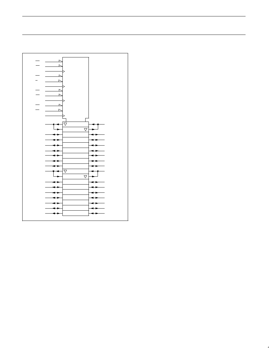
DESCRIPTION
The 74ALVCH16952 consists of two sections, each containing a
dual octal non-inverting registered transceiver. Two 8-bit back to
back registers store data flowing in both directions between two
bi-directional busses. Data applied to the inputs is entered and
stored on the rising edge of the clock (CP
XX
, where X is AB or BA)
provided that the clock enable (CE
XX
) is LOW. The data is then
present at the 3-State output buffers, but is only accessible when the
output enable input (OE
XX
) is LOW. Data flow from A inputs to B
outputs is the same as for B inputs to A outputs.
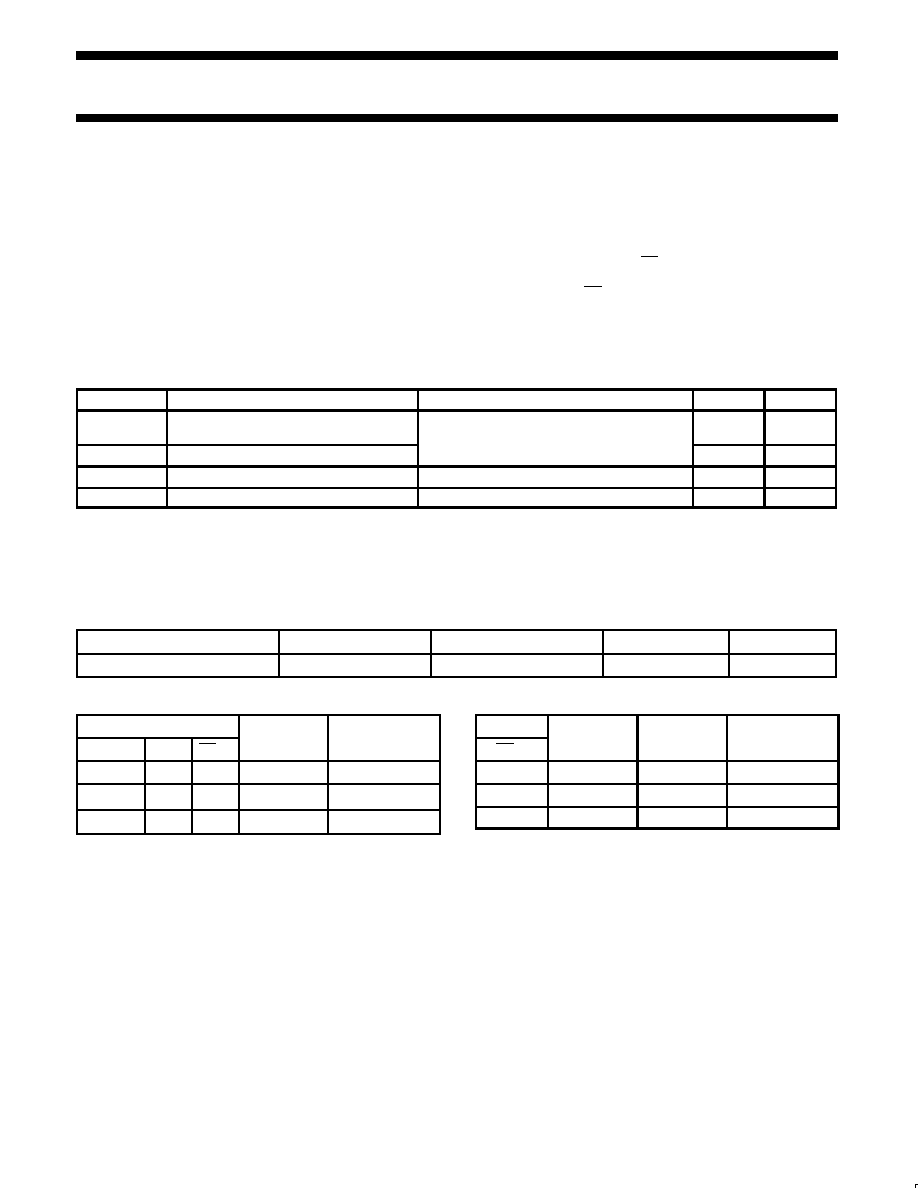
QUICK REFERENCE DATA
GND = 0V; T
amb
= 25
∞
C; t
r
= t
f
= 2.5ns
SYMBOL
PARAMETER
CONDITIONS
TYPICAL
UNIT
t
PHL
/t
PLH
Propagation delay
CPnn, to An, Bn
V
CC
= 3.3V, C
L
= 50pF
V
2 5V C
30pF
3.2
ns
f
MAX
Maximum clock frequency
V
CC
= 2.5V, C
L
= 30pF
350
MHz
C
I
Input capacitance
3.0
pF
C
PD
Power dissipation capacitance per buffer
V
I
= GND to V
CC
1
30
pF
NOTES:
1. C
PD
is used to determine the dynamic power dissipation (P
D
in
µ
W):
P
D
= C
PD
◊
V
CC
2
◊
f
i
+
S
(C
L
◊
V
CC
2
◊
f
o
) where:
f
i
= input frequency in MHz; C
L
= output load capacity in pF;
f
o
= output frequency in MHz; V
CC
= supply voltage in V;
S
(C
L
◊
V
CC
2
◊
f
o
) = sum of outputs.
ORDERING INFORMATION
PACKAGES
TEMPERATURE RANGE
OUTSIDE NORTH AMERICA
NORTH AMERICA
DWG NUMBER
56-Pin Plastic TSSOP Type II
≠40
∞
C to +85
∞
C
74ALVCH16952 DGG
ACH16952 DGG
SOT364-1
FUNCTION TABLE for register An or Bn
INPUTS
INTERNAL
OPERATING
An or Bn
CP
XX
CE
XX
Q
MODE
X
X
H
NC
Hold data
L
∞
L
L
Load data
H
∞
L
H
Load data
H = HIGH voltage level
L = LOW voltage level
= LOW-to-HIGH transition
FUNCTION TABLE for output enable
INPUTS
INTERNAL
An or Bn
OPERATING
OE
nn
Q
OUTPUTS
MODE
H
X
Z
Disable outputs
L
L
L
Enable outputs
L
H
H
Enable outputs
NC = no change
X = don't care
Z = high impedance OFF-state