DATA SHEET
Product specification
Supersedes data of 1998 Dec 11
File under Integrated Circuits, IC24
1999 Nov 15
INTEGRATED CIRCUITS
74AVC16244
16-bit buffer/line driver; 3-state
(3.6 V tolerant)
1999 Nov 15
2
Philips Semiconductors
Product specification
16-bit buffer/line driver; 3-state
(3.6 V tolerant)
74AVC16244
FEATURES
∑
Wide supply voltage range from 1.2 to 3.6 V
∑
Complies with JEDEC standard no. 8-1A/5/7
∑
CMOS low power consumption
∑
Input/output tolerant up to 3.6 V
∑
Dynamic Controlled Output (DCO) circuit dynamically
changes output impedance, resulting in noise reduction
without speed degradation
∑
Low inductance multiple power and ground pins for
minimum noise and ground bounce
∑
Power off disables 74AVC16244 outputs, permitting live
insertion.
DESCRIPTION
The 74AVC16244 is a 16-bit non-inverting buffer/line
driver with 3-state outputs. This device can be used as four
4-bit buffers, two 8-bit buffers or one 16-bit buffer.
The 3-state outputs are controlled by the output enable
inputs nOE. A HIGH level on input nOE causes the outputs
to assume a high-impedance OFF-state.
This product is designed to have an extremely fast
propagation delay and a minimum amount of power
consumption.
To ensure the high-impedance output state during
power-up or power-down, input nOE should be tied to V
CC
through a pull-up resistor (live insertion).
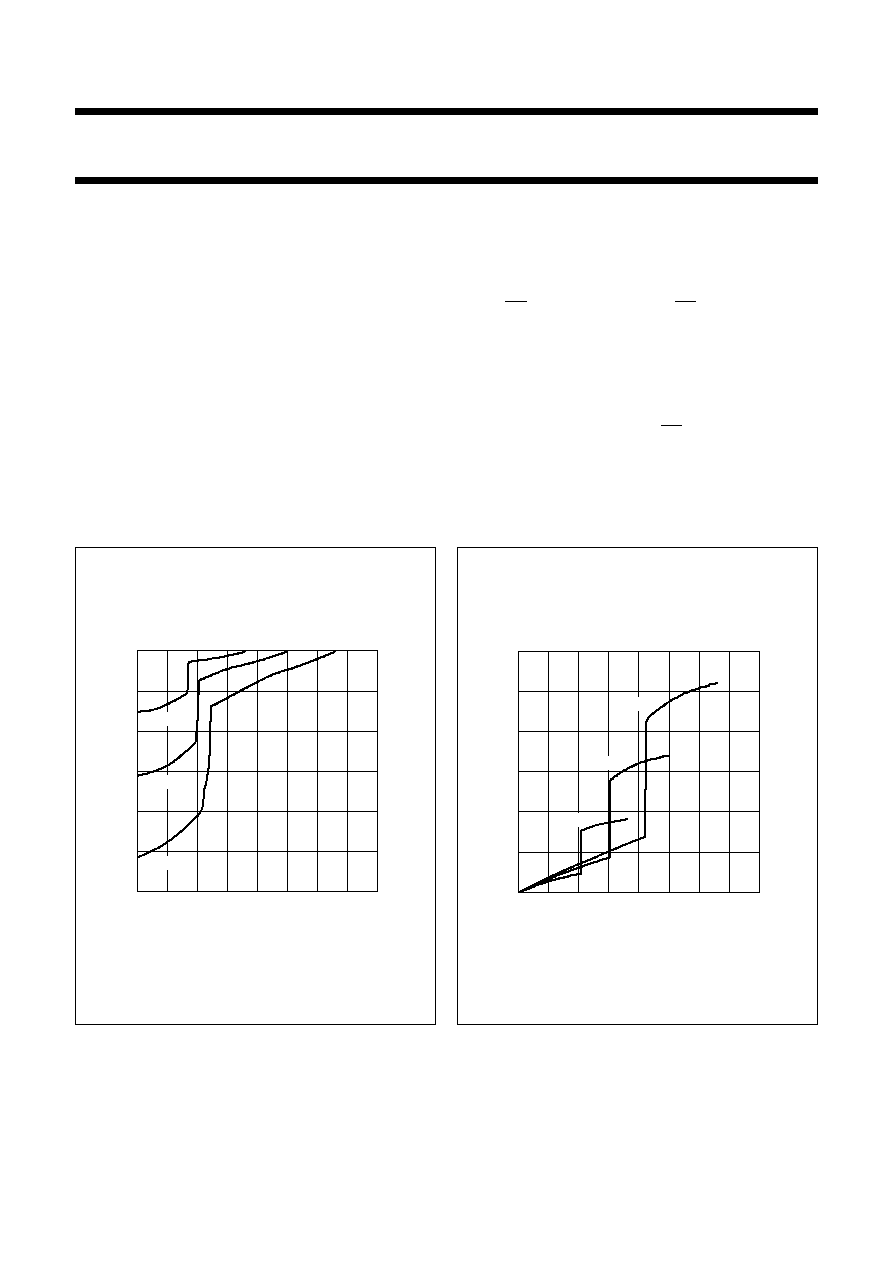
A DCO circuitry is implemented to support termination line
drive during transient (see Figs 1 and 2).
handbook, halfpage
0
1
2
4
0
-
200
-
300
-
100
MNA506
3
VOH (V)
IOH
(mA)
1.8 V
2.5 V
3.3 V
Fig.1 Output current as a function of output voltage.
Fig.2 Output current as a function of output voltage.
handbook, halfpage
0
1
2
4
300
100
0
200
MNA507
3
VOL (V)
IOL
(mA)
1.8 V
2.5 V
3.3 V
1999 Nov 15
3
Philips Semiconductors
Product specification
16-bit buffer/line driver; 3-state
(3.6 V tolerant)
74AVC16244
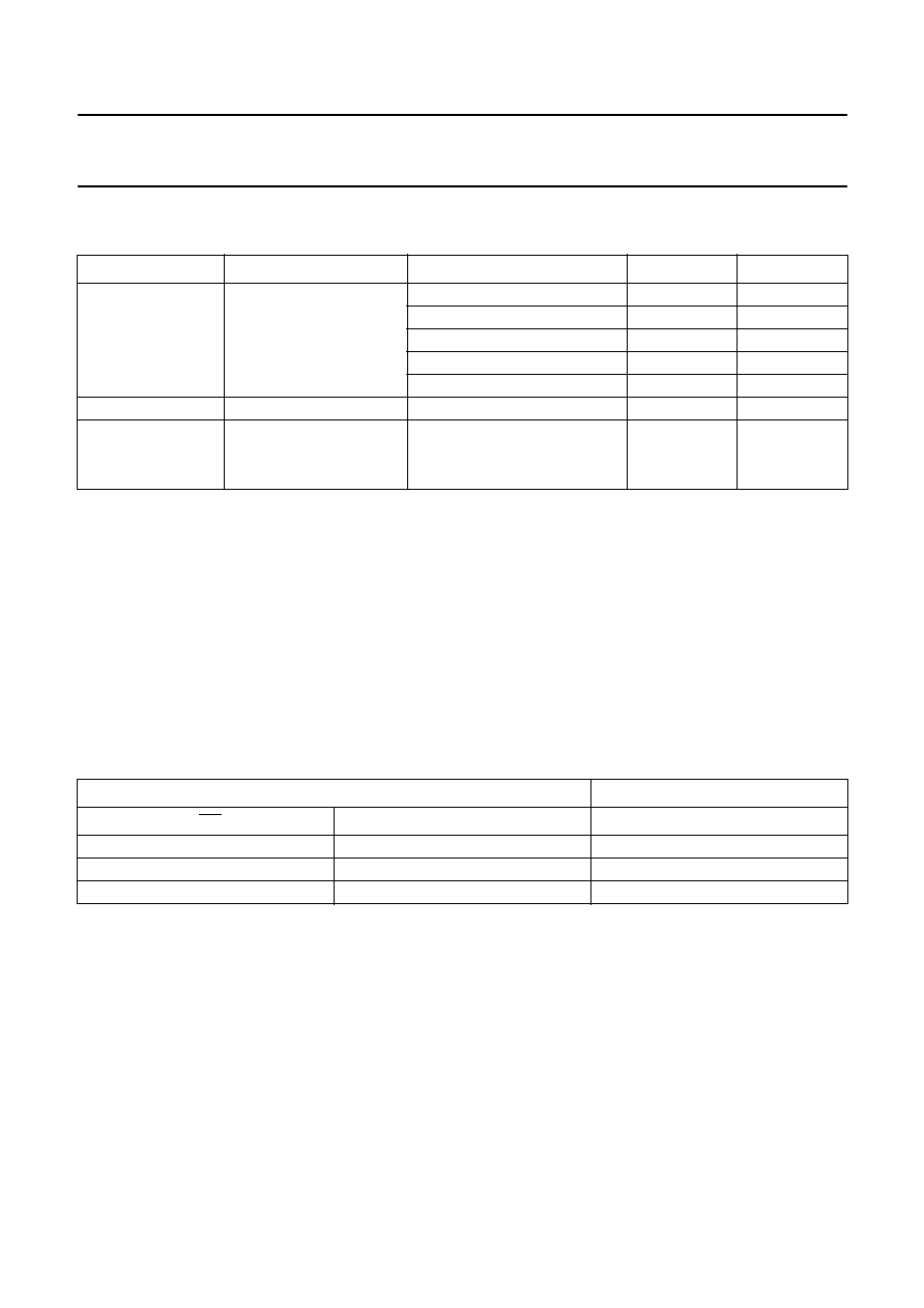
QUICK REFERENCE DATA
GND = 0 V; T
amb
= 25
∞
C; t
r
= t
f
2.0 ns; C
L
= 30 pF.
Notes
1. C
PD
is used to determine the dynamic power dissipation (P
D
in
µ
W).
P
D
= C
PD
◊
V
CC
2
◊
f
i
+
(C
L
◊
V
CC
2
◊
f
o
) where:
f
i
= input frequency in MHz;
f
o
= output frequency in MHz;
C
L
= output load capacitance in pF;
V
CC
= supply voltage in Volts;
(C
L
◊
V
CC
2
◊
f
o
) = sum of outputs.
2. The condition is V
I
= GND to V
CC
.
FUNCTION TABLE
See note 1.
Note
1. H = HIGH voltage level;
L = LOW voltage level;
X = don't care;
Z = high-impedance OFF-state.
SYMBOL
PARAMETER
CONDITIONS
TYP.
UNIT
t
PHL
/t
PLH
propagation delay
nA
n
to nY
n
V
CC
= 1.2 V
2.6
ns
V
CC
= 1.5 V
1.8
ns
V
CC
= 1.8 V
1.7
ns
V
CC
= 2.5 V
1.3
ns
V
CC
= 3.3 V
1.1
ns
C
I
input capacitance
5.0
pF
C
PD
power dissipation
capacitance per buffer
notes 1 and 2
outputs enabled
34
pF
outputs disabled
1
pF
INPUTS
OUTPUTS
nOE
nA
n
nY
n
L
L
L
L
H
H
H
X
Z
1999 Nov 15
4
Philips Semiconductors
Product specification
16-bit buffer/line driver; 3-state
(3.6 V tolerant)
74AVC16244
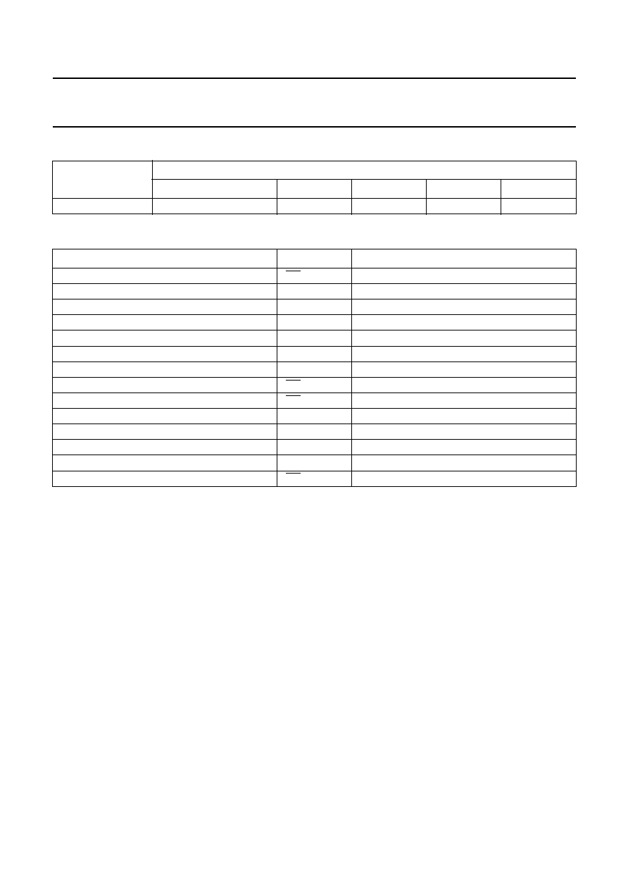
ORDERING INFORMATION
PINNING
TYPE NUMBER
PACKAGE
TEMPERATURE RANGE
PINS
PACKAGE
MATERIAL
CODE
74AVC16244DGG
-
40 to +85
∞
C
48
TSSOP
plastic
SOT362-1
PIN
SYMBOL
DESCRIPTION
1
1OE
output enable input (active LOW)
2, 3, 5 and 6
1Y
0
to 1Y
3
data outputs
4, 10, 15, 21, 28, 34, 39 and 45
GND
ground (0 V)
7, 18, 31 and 42
V
CC
positive supply voltage
8, 9, 11 and 12
2Y
0
to 2Y
3
data outputs
13, 14, 16 and 17
3Y
0
to 3Y
3
data outputs
19, 20, 22 and 23
4Y
0
to 4Y
3
data outputs
24
4OE
output enable input (active LOW)
25
3OE
output enable input (active LOW)
26, 27, 29 and 30
4A
3
to 4A
0
data inputs
32, 33, 35 and 36
3A
3
to 3A
0
data inputs
37, 38, 40 and 41
2A
3
to 2A
0
data inputs
43, 44, 46 and 47
1A
3
to 1A
0
data inputs
48
2OE
output enable input (active LOW)
1999 Nov 15
5
Philips Semiconductors
Product specification
16-bit buffer/line driver; 3-state
(3.6 V tolerant)
74AVC16244
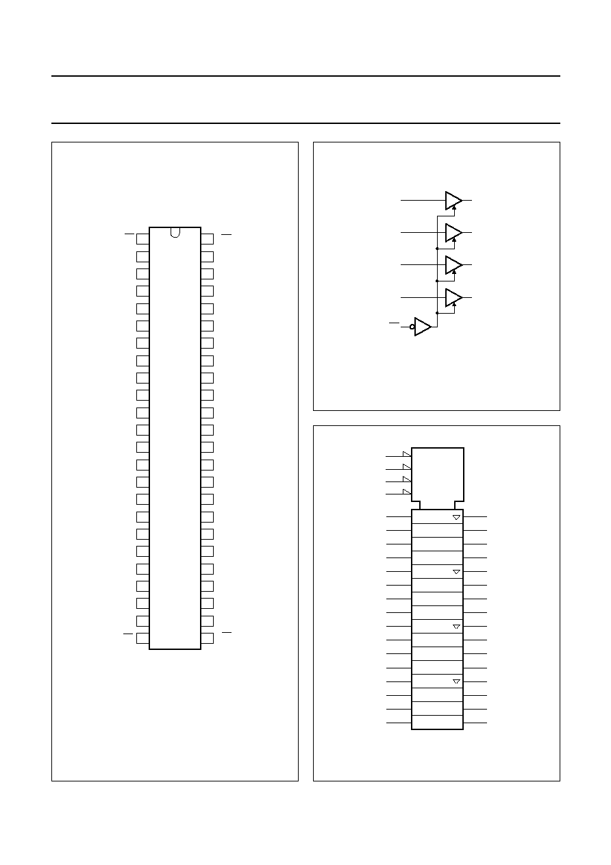
Fig.3 Pin configuration.
handbook, halfpage
16244
MNA501
1
2
3
4
5
6
7
8
9
10
11
12
13
14
15
16
17
18
19
20
21
22
23
24
26
25
48
47
46
45
44
43
42
41
40
39
38
37
36
35
34
33
32
31
30
29
28
27
1Y0
1Y1
GND
1Y2
1Y3
VCC
2Y0
2Y1
GND
2Y2
2Y3
3Y0
3Y1
GND
3Y2
3Y3
VCC
4Y0
4Y1
GND
4Y2
4Y3
4OE
1A0
1A1
GND
1A2
1A3
VCC
2A0
2A1
GND
2A2
2A3
3A0
3A1
GND
3A2
3A3
VCC
4A0
4A1
GND
4A2
4A3
3OE
1OE
2OE
handbook, halfpage
MNA502
nA3
nA2
nA1
nA0
nY0
nY1
nY2
nY3
nOE
Fig.4 Logic symbol.
handbook, halfpage
23
MNA503
37
12
11
9
8
6
5
47
46
44
43
41
40
38
2
3
26
22
20
19
17
16
36
35
33
32
30
29
27
13
14
24
4EN
25
3EN
1
1EN
48
2EN
1
1
3
1
2
1
4
1
Fig.5 IEEE/IEC logic symbol.