 | –≠–ª–µ–∫—Ç—Ä–æ–Ω–Ω—ã–π –∫–æ–º–ø–æ–Ω–µ–Ω—Ç: 74F3893A | –°–∫–∞—á–∞—Ç—å:  PDF PDF  ZIP ZIP |
Document Outline
- FEATURES
- DESCRIPTION
- ORDERING INFORMATION
- INPUT AND OUTPUT LOADING AND FAN OUT TABLE
- PIN CONFIGURATION
- FUNCTION TABLE
- LOGIC SYMBOL
- LOGIC DIAGRAM
- IEC/IEEE SYMBOL
- ABSOLUTE MAXIMUM RATINGS
- RECOMMENDED OPERATING CONDITIONS
- DC ELECTRICAL CHARACTERISTICS
- AC ELECTRICAL CHARACTERISTICS
- AC WAVEFORMS
- TEST CIRCUITS AND WAVEFORMS
- PACKAGE OUTLINE
- Data sheet status
- Definitions
- Disclaimers

Philips
Semiconductors
74F3893
Quad futurebus backplane transceiver
Product specification
IC15 Data Handbook
1991 Jan 18
INTEGRATED CIRCUITS

Philips Semiconductors
Product specification
74F3893
Quad Futurebus backplane transceiver
2
January 18, 1991
853-1397 01496
FEATURES
∑
Quad backplane transceiver
∑
Drives heavily loaded backplanes with equivalent load
impedances down to 10 ohms
∑
Futurebus drivers sink 100mA
∑
Reduced voltage swing (1 volt) produces less noise and
reduces power consumption
∑
High speed operation enhances performance of backplane
buses and facilitates incident wave switching
∑
Compatible with IEEE 896 and IEEE 1194.1 Futurebus
Standards
∑
Built≠in precision band≠gap (BG) reference provides
accurate receiver thresholds and improved noise immunity
∑
Glitch≠free power up/power down operation on all outputs
∑
Pin and function compatible with NSC DS3893
DESCRIPTION
The 74F3893 is a quad backplane transceivers and is
intended to be used in very high speed bus systems.
The 74F3893 interfaces to `Backplane Transceiver Logic'
(BTL). BTL features a reduced (1V to 2V) voltage swing for
lower power consumption and a series diode on the drivers
to reduce capacitive loading (< 5pF).
Incident wave switching is employed, therefore BTL
propagation delays are short. Although the voltage swing is
much less for BTL, so is its receiver threshold region,
therefore noise margins are excellent.
BTL offers low power consumption, low ground bounce, EMI
and crosstalk, low capacitive loading, superior noise margin
and low propagation delays. This results in a high
bandwidth, reliable backplane.
T
he 74F3893 has four TTL outputs (Rn) on the receiver
side with a common receiver enable input (RE). It has four
data inputs (Dn) which are also TTL. These data inputs are
NANDed with the data enable input (DE). The four I/O pins
(bus side) are futurebus compatible, sink a minimum of
100mA, and are designed to drive heavily loaded
backplanes with load impedances as low as 10 ohms. All
outputs are designed to be glitch≠free during power up and
down.
TYPE
TYPICAL
PROPAGATION DELAY
TYPICAL SUPPLY
CURRENT( TOTAL)
74F3893
3.0ns
55mA
ORDERING INFORMATION
ORDER CODE
DESCRIPTION
COMMERCIAL RANGE
V
CC
= 5V
±
10%,
T
amb
= 0
∞
C to +70
∞
C
PKG DWG #
20-pin PLCC
N74F3893A
SOT380-1
INPUT AND OUTPUT LOADING AND FAN OUT TABLE
PINS
DESCRIPTION
74F (U.L.)
HIGH/LOW
LOAD VALUE
HIGH/LOW
D0 ≠ D3
Data inputs
1.0/0.067
20
µ
A/40
µ
A
DE
Data enable input
1.0/0.33
20
µ
A/200
µ
A
RE
Receiver enable input
1.0/0.067
20
µ
A/40
µ
A
I/O0 ≠ I/O3
Bus inputs
5.0/0.033
100
µ
A/20
µ
A
I/O0 ≠ I/O3
Bus outputs
OC/166.7
OC/100mA
R0 ≠ R7
Receiver outputs
150/40
3mA/24mA
Notes to input and output loading and fan out table
One (1.0) FAST unit load is defined as: 20
µ
A in the high state and 0.6mA in the low state.
OC= Open collector.
Philips Semiconductors
Product specification
74F3893
Quad Futurebus backplane transceiver
January 18, 1991
3
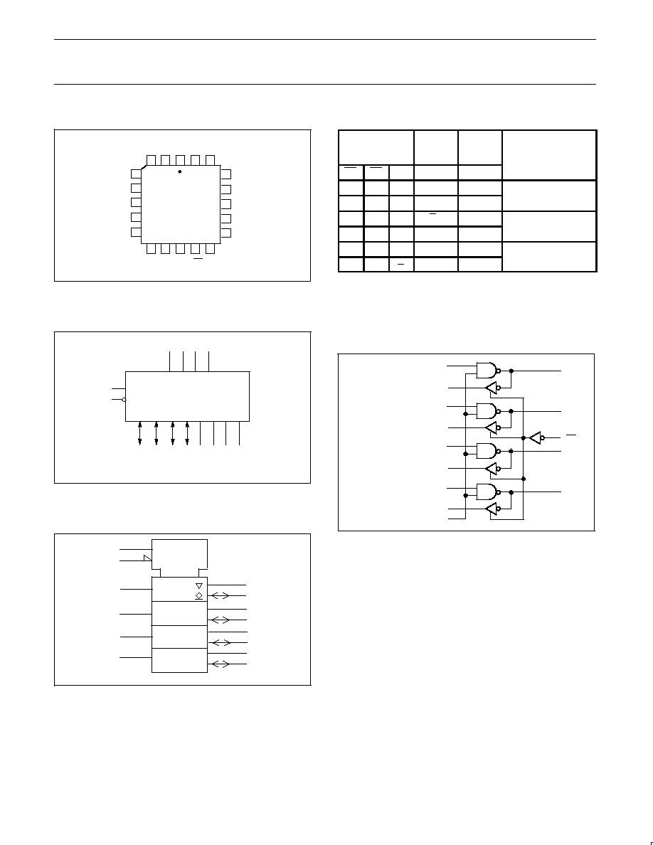
PIN CONFIGURATION
3
2
1
20
19
18
17
16
15
14
8
7
6
5
13
12
11
10
9
4
PLCC
D1
R1
LOGIC GND
D2
R2
VCC
BG
GND
D0
R0
RE
DE
R3
D3
I/O0
I/O1
BUS GND
I/O2
I/O3
BUS
GND
BUS
GND
SF00573
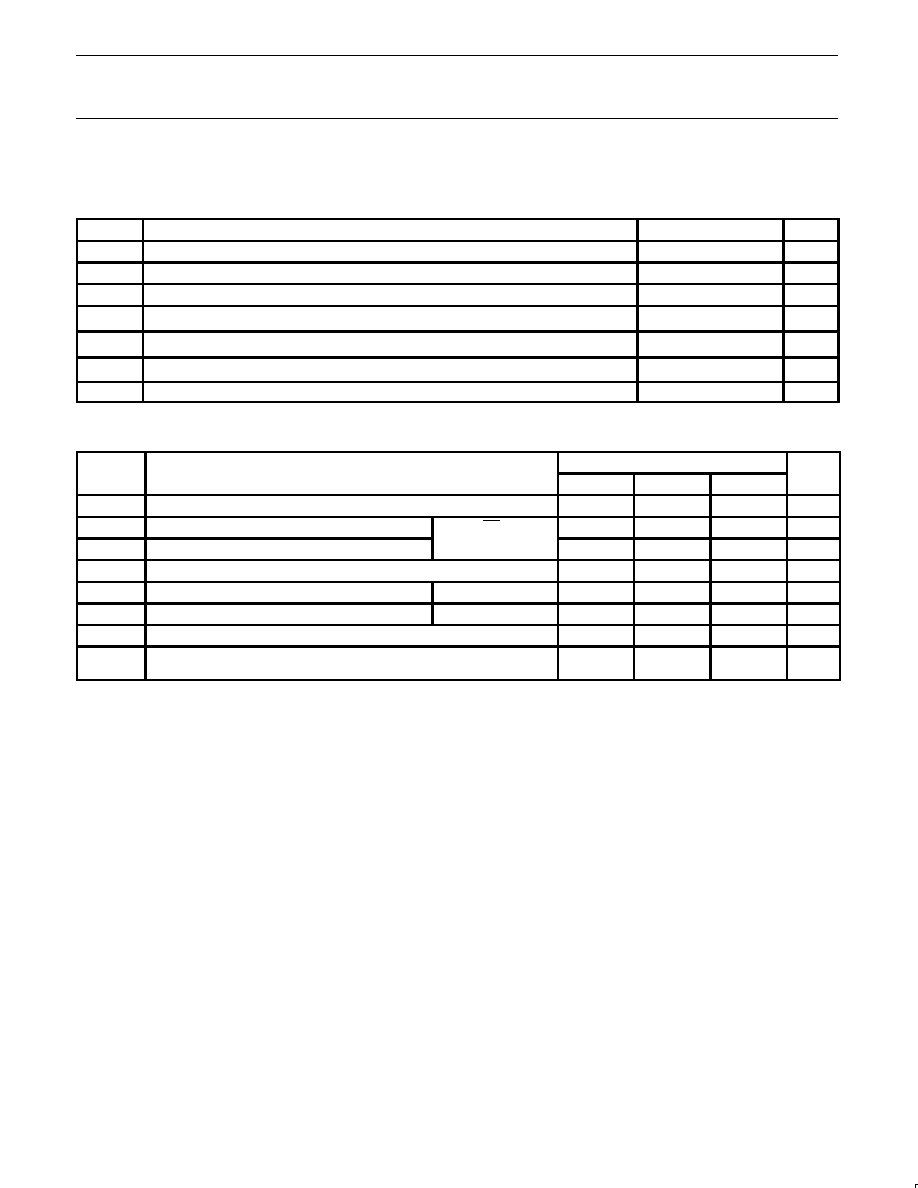
LOGIC SYMBOL
DE
RE
2 4 7 9
D0 D1 D2 D3
I/O0 I/O1 1/O2 I/O3
R0 R1 R2 R3
V
CC
= Pin 1,
LOGIC GND = Pin 8
BUS GND = Pin 13, 16, 19
BG GND = Pin 20
18 17 15 14
3 5 8 10
11
12
SF00574
IEC/IEEE SYMBOL
2
1D
3
18
5
17
7
15
9
14
2
4
7
9
11
12
EN1
EN2
SF00575
FUNCTION TABLE
INPUTS
INPUT/
OUT-
PUT
OUT-
PUT
OPERATING
DE
RE
Dn
I/On
Rn
MODE
H
L
L
H
L
Transmit to bus
H
L
H
L
H
H
H
Dn
Dn
Z
Receiver 3≠state,
L
H
X
H
Z
transmit to bus
L
L
X
H
L
Receive, I/On = inputs
L
L
X
L
H
Notes to function table
1. H = High voltage level
2. L
= Low voltage level
3. X = Don't care
4. Z = High impedance "off" state
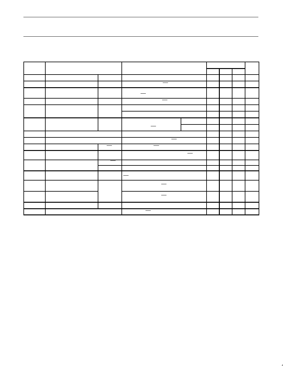
LOGIC DIAGRAM
V
CC
= Pin 1
LOGIC GND = Pin 6
BUS GND = Pin 13, 16, 19
BG GND = Pin 20
2
3
5
8
10
18
12
14
D0
R0
R1
R2
R3
I/O0
RE
I/O3
SF00576
D1
4
7
9
11
D2
D3
DE
I/O2
15
I/O1
17
Philips Semiconductors
Product specification
74F3893
Quad Futurebus backplane transceiver
January 18, 1991
4
ABSOLUTE MAXIMUM RATINGS
(Operation beyond the limit set forth in this table may impair the useful life of the device. Unless otherwise noted these limits are over the
operating free air temperature range.)
SYMBOL
PARAMETER
RATING
UNIT
V
CC
Supply voltage
≠1.5 to +6.5
V
V
IN
Input voltage
≠1.5 to +6.5
V
I
IN
Input current
≠30 to +5
mA
V
OUT
Voltage applied to output in high output state
≠0.5 to 5.5
V
I
OUT
Current applied to output in low output state
200
mA
T
amb
Operating free air temperature range
0 to +70
∞
C
T
stg
Storage temperature range
≠65 to +150
∞
C
RECOMMENDED OPERATING CONDITIONS
LIMITS
SYMBOL
PARAMETER
MIN
NOM
MAX
UNIT
V
CC
Supply voltage
4.5
5.0
5.5
V
V
IH
High≠level input voltage
Dn, DE, RE
2.0
V
V
IL
Low≠level input voltage
0.8
V
I
Ik
Input clamp current
≠18
mA
V
TH
Bus input threshold
I/On only
1.475
1.55
1.625
mA
I
OH
High≠level output current
Rn only
≠3
mA
I
OL
Low≠level output current
100
mA
T
amb
Operating free air temperature
range
0
+70
∞
C
Philips Semiconductors
Product specification
74F3893
Quad Futurebus backplane transceiver
January 18, 1991
5
DC ELECTRICAL CHARACTERISTICS
(Over recommended operating free-air temperature range unless otherwise noted.)
SYMBOL
PARAMETER
TEST
LIMITS
UNIT
CONDITIONS
1
MIN
TYP
2
MAX
I
OH
High≠level output current
I/On
V
CC
= MAX, V
IL
= MAX, V
IH
= MIN, V
OH
= 1.5V
10
100
µ
A
V
OH
High-level output voltage
Rn
V
CC
= MAX, V
IL
= 1.3V, RE = 0.8V, I
OH
= MAX
2.5
V
V
OHB
High-level output bus voltage
I/On
V
CC
= MAX, Dn = DE = 0.8V, V
T
= 2.0V,
R
T
= 10
, RE = 2.0V
2.5
V
V
OL
Low-level output voltage
Rn
V
CC
= MIN, V
IN
= 1.8V, RE = 0.8V, I
OL
= 6mA
0.35
0.5
V
V
OLB
Low-level output
I/On
Dn = DE = V
IH
, I
OL
= 100mA
0.75
1.0
1.2
V
bus voltage
Dn = DE = V
IH
, I
OL
= 80mA
0.75
1.0
1.1
V
V
OCB
Driver output positive
I/On
V
CC
= MAX or 0V,
I/On = 1mA
1.9
2.9
V
clamp voltage
Dn = DE = 0.8V, RE = 2.0V
I/On = 10mA
2.3
3.2
V
V
IK
Input clamp voltage
V
CC
= MIN, I
I
=I
IK
≠0.73
-1.2
V
I
I
Input current at maximum input voltage
V
CC
= MAX, V
I
= 7.0V, DE = RE = Dn = V
CC
100
µ
A
I
IH
High≠level input current
Dn, RE, DE
V
CC
= MAX, DE = RE = Dn =5.5V
20
µ
A
I
IHB
High≠level I/O bus current
(power off)
I/On
V
CC
= 0V, Dn = DE = 0.8V, I/On =1.2V, RE = 0V
100
µ
A
I
IL
Low≠level input current
Dn, RE
V
CC
= MAX, V
I
= 0.5V, DE = 4.5V
≠40
µ
A
DE
V
CC
= MAX, V
I
= 0.5V, Dn = 4.5V
≠200
µ
A
I
ILB
Low≠level I/O bus current
(power on)
I/On
V
CC
= MAX, Dn = DE = 0.8V, I/On =0.75V,
RE = 0V
≠20
20
µ
A
I
OZH
Off≠state output current,
high≠level voltage applied
Rn
V
CC
= MAX, V
I
= 2.7V, RE = 2V
20
µ
A
I
OZL
Off≠state output current,
low≠level voltage applied
V
CC
= MAX, V
I
= 0.5V, RE = 2V
≠20
µ
A
I
OS
Short circuit output current
3
Rn
'F8
V
CC
= MAX
-60
-150
mA
I
CC
Supply current
4
(total)
V
CC
= MAX, (RE = V
IH
or V
IL
)
55
80
mA
Notes to DC electrical characteristics
1. For conditions shown as MIN or MAX, use the appropriate value specified under recommended operating conditions for the applicable type.
2. All typical values are at V
CC
= 5V, T
amb
= 25
∞
C.
3. Not more than one output should be shorted at a time. For testing I
OS
, the use of high-speed test apparatus and/or sample-and-hold
techniques are preferable in order to minimize internal heating and more accurately reflect operational values. Otherwise, prolonged shorting
of a high output may raise the chip temperature well above normal and thereby cause invalid readings in other parameter tests. In any
sequence of parameter tests, I
OS
tests should be performed last.