 | –≠–ª–µ–∫—Ç—Ä–æ–Ω–Ω—ã–π –∫–æ–º–ø–æ–Ω–µ–Ω—Ç: 74HC132N | –°–∫–∞—á–∞—Ç—å:  PDF PDF  ZIP ZIP |

DATA SHEET
Product specification
File under Integrated Circuits, IC06
September 1993
INTEGRATED CIRCUITS
74HC/HCT132
Quad 2-input NAND Schmitt trigger
For a complete data sheet, please also download:
∑
The IC06 74HC/HCT/HCU/HCMOS Logic Family Specifications
∑
The IC06 74HC/HCT/HCU/HCMOS Logic Package Information
∑
The IC06 74HC/HCT/HCU/HCMOS Logic Package Outlines

September 1993
2
Philips Semiconductors
Product specification
Quad 2-input NAND Schmitt trigger
74HC/HCT132
FEATURES
∑
Output capability: standard
∑
I
CC
category: SSI
GENERAL DESCRIPTION
The 74HC/HCT132 are high-speed Si-gate CMOS devices and are pin compatible with low power Schottky TTL (LSTTL).
They are specified in compliance with JEDEC standard no. 7A.
The 74HC/HCT132 contain four 2-input NAND gates which accept standard input signals. They are capable of
transforming slowly changing input signals into sharply defined, jitter-free output signals.
The gate switches at different points for positive and negative-going signals. The difference between the positive voltage
V
T
+
and the negative voltage V
T
-
is defined as the hysteresis voltage V
H
.
QUICK REFERENCE DATA
GND = 0 V; T
amb
= 25
∞
C; t
r
= t
f
= 6 ns
Notes
1. C
PD
is used to determine the dynamic power dissipation (P
D
in
µ
W):
P
D
= C
PD
◊
V
CC
2
◊
f
i
+
(C
L
◊
V
CC
2
◊
f
o
) where:
f
i
= input frequency in MHz
f
o
= output frequency in MHz
(C
L
◊
V
CC
2
◊
f
o
) = sum of outputs
C
L
= output load capacitance in pF
V
CC
= supply voltage in V
2. For HC the condition is V
I
= GND to V
CC
For HCT the condition is V
I
= GND to V
CC
-
1.5 V
ORDERING INFORMATION
See
"74HC/HCT/HCU/HCMOS Logic Package Information"
.
SYMBOL
PARAMETER
CONDITIONS
TYPICAL
UNIT
HC
HCT
t
PHL
/ t
PLH
propagation delay nA, nB to nY
C
L
= 15 pF; V
CC
= 5 V 11
17
ns
C
I
input capacitance
3.5
3.5
pF
C
PD
power dissipation capacitance per gate
notes 1 and 2
24
20
pF

September 1993
3
Philips Semiconductors
Product specification
Quad 2-input NAND Schmitt trigger
74HC/HCT132
PIN DESCRIPTION
PIN NO.
SYMBOL
NAME AND FUNCTION
1, 4, 9, 12
1A to 4A
data inputs
2, 5, 10, 13
1B to 4B
data inputs
3, 6, 8, 11
1Y to 4Y
data outputs
7
GND
ground (0 V)
14
V
CC
positive supply voltage
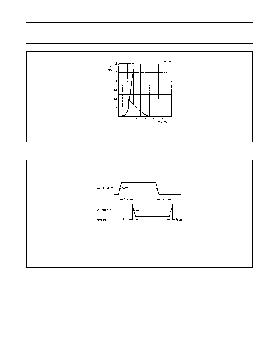
Fig.1 Pin configuration.
Fig.2 Logic symbol.
Fig.3 IEC logic symbol.
Fig.4 Functional diagram.
Fig.5
Logic diagram
(one Schmitt trigger).
FUNCTION TABLE
Notes
1. H = HIGH voltage level
L = LOW voltage level
APPLICATIONS
∑
Wave and pulse shapers
∑
Astable multivibrators
∑
Monostable multivibrators
INPUTS
OUTPUT
nA
nB
nY
L
L
H
L
H
H
H
L
H
H
H
L

September 1993
4
Philips Semiconductors
Product specification
Quad 2-input NAND Schmitt trigger
74HC/HCT132
DC CHARACTERISTICS FOR 74HC
For the DC characteristics see
"74HC/HCT/HCU/HCMOS Logic Family Specifications"
. Transfer characteristics are
given below.
Output capability: standard
I
CC
category: SSI
Transfer characteristics for 74HC
Voltages are referenced to GND (ground = 0 V)
AC CHARACTERISTICS FOR 74HC
GND = 0 V; t
r
= t
f
= 6 ns; C
L
= 50 pF
SYMBOL PARAMETER
T
amb
(
∞
C)
UNIT
TEST CONDITIONS
74HC
V
CC
(V)
WAVEFORMS
+
25
-
40 to
+
85
-
40 to
+
125
min.
typ.
max.
min.
max.
min.
max.
V
T
+
positive-going threshold
0.7
1.18
1.5
0.7
1.5
0.7
1.5
V
2.0
Figs 6 and 7
1.7
2.38
3.15
1.7
3.15
1.7
3.15
4.5
2.1
3.14
4.2
2.1
4.2
2.1
4.2
6.0
V
T
-
negative-going threshold 0.3
0.63
1.0
0.3
1.0
0.3
1.0
V
2.0
Figs 6 and 7
0.9
1.67
2.2
0.9
2.2
0.9
2.2
4.5
1.2
2.26
3.0
1.2
3.0
1.2
3.0
6.0
V
H
hysteresis (V
T
+
-
V
T
-
)
0.2
0.55
1.0
0.2
1.0
0.2
1.0
V
2.0
Figs 6 and 7
0.4
0.71
1.4
0.4
1.4
0.4
1.4
4.5
0.6
0.88
1.6
0.6
1.6
0.6
1.6
6.0
SYMBOL
PARAMETER
T
amb
(
∞
C)
UNIT
TEST CONDITIONS
74HC
V
CC
(V)
WAVEFORMS
+
25
-
40 TO
+
85
-
40 TO
+
125
min.
typ.
max.
min.
max.
min.
max.
t
PHL
/ t
PLH
propagation delay
nA, nB to nY
36
125
155
190
ns
2.0
Fig.13
13
25
31
38
4.5
10
21
26
32
6.0
t
THL
/ t
TLH
output transition time
19
75
95
110
ns
2.0
Fig.13
7
15
19
22
4.5
6
13
16
19
6.0

September 1993
5
Philips Semiconductors
Product specification
Quad 2-input NAND Schmitt trigger
74HC/HCT132
DC CHARACTERISTICS FOR 74HCT
For the DC characteristics see
"74HC/HCT/HCU/HCMOS Logic Family Specifications"
. Transfer characteristics are
given below.
Output capability: standard
I
CC
category: SSI
Notes to HCT types
The value of additional quiescent supply current (
I
CC
) for a unit load of 1 is given in the family specifications.
To determine
I
CC
per input, multiply this value by the unit load coefficient shown in the table below.
Transfer characteristics for 74HCT
Voltages are referenced to GND (ground = 0 V)
AC CHARACTERISTICS FOR 74HCT
GND = 0 V; t
r
= t
f
= 6 ns; C
L
= 50 pF
INPUT
UNIT LOAD COEFFICIENT
nA, nB
0.3
SYMBOL PARAMETER
T
amb
(
∞
C)
UNIT
TEST CONDITIONS
74HCT
V
CC
(V)
WAVEFORMS
+
25
-
40 to
+
85
-
40 to
+
125
min.
typ.
max.
min.
max.
min.
max.
V
T
+
positive-going threshold
1.2
1.41
1.9
1.2
1.9
1.2
1.9
V
4.5
Figs 6 and 7
1.4
1.59
2.1
1.4
2.1
1.4
2.1
5.5
V
T
-
negative-going threshold 0.5
0.85
1.2
0.5
1.2
0.5
1.2
V
4.5
Figs 6 and 7
0.6
0.99
1.4
0.6
1.4
0.6
1.4
5.5
V
H
hysteresis (V
T
+
-
V
T
-
)
0.4
0.56
-
0.4
-
0.4
-
V
4.5
Figs 6 and 7
0.4
0.60
-
0.4
-
0.4
-
5.5
SYMBOL
PARAMETER
T
amb
(
∞
C)
UNIT
TEST CONDITIONS
74HCT
V
CC
(V)
WAVEFORMS
+
25
-
40 to
+
85
-
40 to
+
125
min.
typ.
max.
min.
max.
min.
max.
t
PHL
/ t
PLH
propagation delay
nA, nB to nY
20
33
41
50
ns
4.5
Fig.13
t
THL
/ t
TLH
output transition time
7
15
19
22
ns
4.5
Fig.13

September 1993
6
Philips Semiconductors
Product specification
Quad 2-input NAND Schmitt trigger
74HC/HCT132
TRANSFER CHARACTERISTIC WAVEFORMS
Fig.6 Transfer characteristic.
Fig.7
Waveforms showing the definition of V
T
+
,
V
T
-
and V
H
; where V
T
+
and V
T
-
are between
limits of 20% and 70%.
Fig.8
Typical HC transfer characteristics;
V
CC
= 2 V.
Fig.9
Typical HC transfer characteristics;
V
CC
= 4.5 V.
Fig.10 Typical HC transfer characteristics;
V
CC
= 6 V.
Fig.11 Typical HCT transfer characteristics;
V
CC
= 4.5 V.
September 1993
7
Philips Semiconductors
Product specification
Quad 2-input NAND Schmitt trigger
74HC/HCT132
AC WAVEFORMS
Fig.12 Typical HCT transfer characteristics; V
CC
= 5.5 V.
Fig.13 Waveforms showing the input (nA, nB) to output (nY) propagation delays and the output transition times.
(1) HC : V
M
= 50%; V
I
= GND to V
CC
.
HCT: V
M
= 1.3 V; V
I
= GND to 3 V.
September 1993
8
Philips Semiconductors
Product specification
Quad 2-input NAND Schmitt trigger
74HC/HCT132
Application information
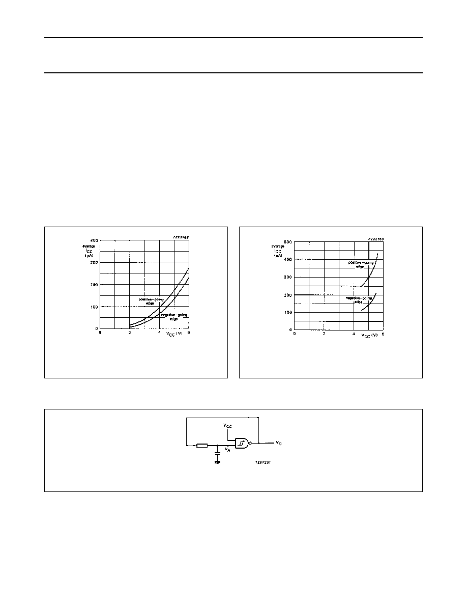
The slow input rise and fall times cause additional power dissipation, this can be calculated using the following formula:
P
ad
= f
i
◊
(t
r
◊
I
CCa
+
t
f
◊
I
CCa
)
◊
V
CC
.
Where:
Average I
CCa
differs with positive or negative input transitions, as shown in Figs 14 and 15.
P
ad
f
i
t
r
t
f
I
CCa
= additional power dissipation (
µ
W)
= input frequency (MHz)
= input rise time (ns); 10%
-
90%
= input fall time (ns); 10%
-
90%
= average additional supply current (
µ
A)
Fig.14 Average I
CC
for HC Schmitt trigger devices;
linear change of V
i
between 0.1 V
CC
to
0.9 V
CC
.
Fig.15 Average I
CC
for HCT Schmitt trigger
devices; linear change of V
i
between
0.1 V
CC
to 0.9 V
CC
.
HC/HCT132 used in a relaxation oscillator circuit, see Fig.16.
Note to Application information
All values given are typical unless otherwise specified.
PACKAGE OUTLINES
See
"74HC/HCT/HCU/HCMOS Logic Package Outlines"
.
Fig.16 Relaxation oscillator using HC/HCT132.
HC:
HCT:
f
1
T
---
1
0.8RC
-----------------
=
f
1
T
---
1
0.67 RC
----------------------
=