DATA SHEET
Product specification
File under Integrated Circuits, IC06
December 1990
INTEGRATED CIRCUITS
74HC/HCT237
3-to-8 line decoder/demultiplexer
with address latches
For a complete data sheet, please also download:
∑
The IC06 74HC/HCT/HCU/HCMOS Logic Family Specifications
∑
The IC06 74HC/HCT/HCU/HCMOS Logic Package Information
∑
The IC06 74HC/HCT/HCU/HCMOS Logic Package Outlines
December 1990
2
Philips Semiconductors
Product specification
3-to-8 line decoder/demultiplexer with
address latches
74HC/HCT237
FEATURES
∑
Combines 3-to-8 decoder with 3-bit latch
∑
Multiple input enable for easy expansion or independent
controls
∑
Active HIGH mutually exclusive outputs
∑
Output capability: standard
∑
I
CC
category: MSI
GENERAL DESCRIPTION
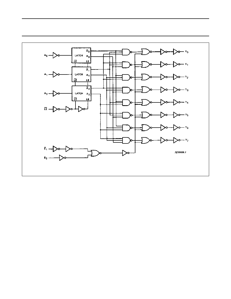
The 74HC/HCT237 are high-speed Si-gate CMOS devices
and are pin compatible with low power Schottky TTL
(LSTTL). They are specified in compliance with JEDEC
standard no. 7A.
The 74HC/HCT237 are 3-to-8 line decoder/demultiplexers
with latches at the three address inputs (A
n
). The "237"
essentially combines the 3-to-8 decoder function with a
3-bit storage latch. When the latch is enabled (LE = LOW),
the "237" acts as a 3-to-8 active LOW decoder. When the
latch enable (LE) goes from LOW-to-HIGH, the last data
present at the inputs before this transition, is stored in the
latches. Further address changes are ignored as long as
LE remains HIGH.
The output enable input (E
1
and E
2
) controls the state of
the outputs independent of the address inputs or latch
operation. All outputs are HIGH unless E
1
is LOW and E
2
is HIGH.
The "237" is ideally suited for implementing
non-overlapping decoders in 3-state systems and strobed
(stored address) applications in bus oriented systems.
QUICK REFERENCE DATA
GND = 0 V; T
amb
= 25
∞
C; t
r
= t
f
= 6 ns
Notes
1. C
PD
is used to determine the dynamic power dissipation (P
D
in
µ
W):
P
D
= C
PD
◊
V
CC
2
◊
f
i
+
(C
L
◊
V
CC
2
◊
f
o
) where:
f
i
= input frequency in MHz
f
o
= output frequency in MHz
(C
L
◊
V
CC
2
◊
f
o
) = sum of outputs
C
L
= output load capacitance in pF
V
CC
= supply voltage in V
2. For HC the condition is V
I
= GND to V
CC
For HCT the condition is V
I
= GND to V
CC
-
1.5 V
ORDERING INFORMATION
See
"74HC/HCT/HCU/HCMOS Logic Package Information"
.
SYMBOL
PARAMETER
CONDITIONS
TYPICAL
UNIT
HC
HCT
t
PHL
/ t
PLH
propagation delay
C
L
= 15 pF; V
CC
= 5 V
A
n
to Y
n
16
19
ns
LE to Y
n
19
21
ns
E
1
to Y
n
14
17
ns
E
2
to Y
n
14
17
ns
C
I
input capacitance
3.5
3.5
pF
C
PD
power dissipation capacitance per package
notes 1 and 2
60
63
pF
December 1990
3
Philips Semiconductors
Product specification
3-to-8 line decoder/demultiplexer with
address latches
74HC/HCT237
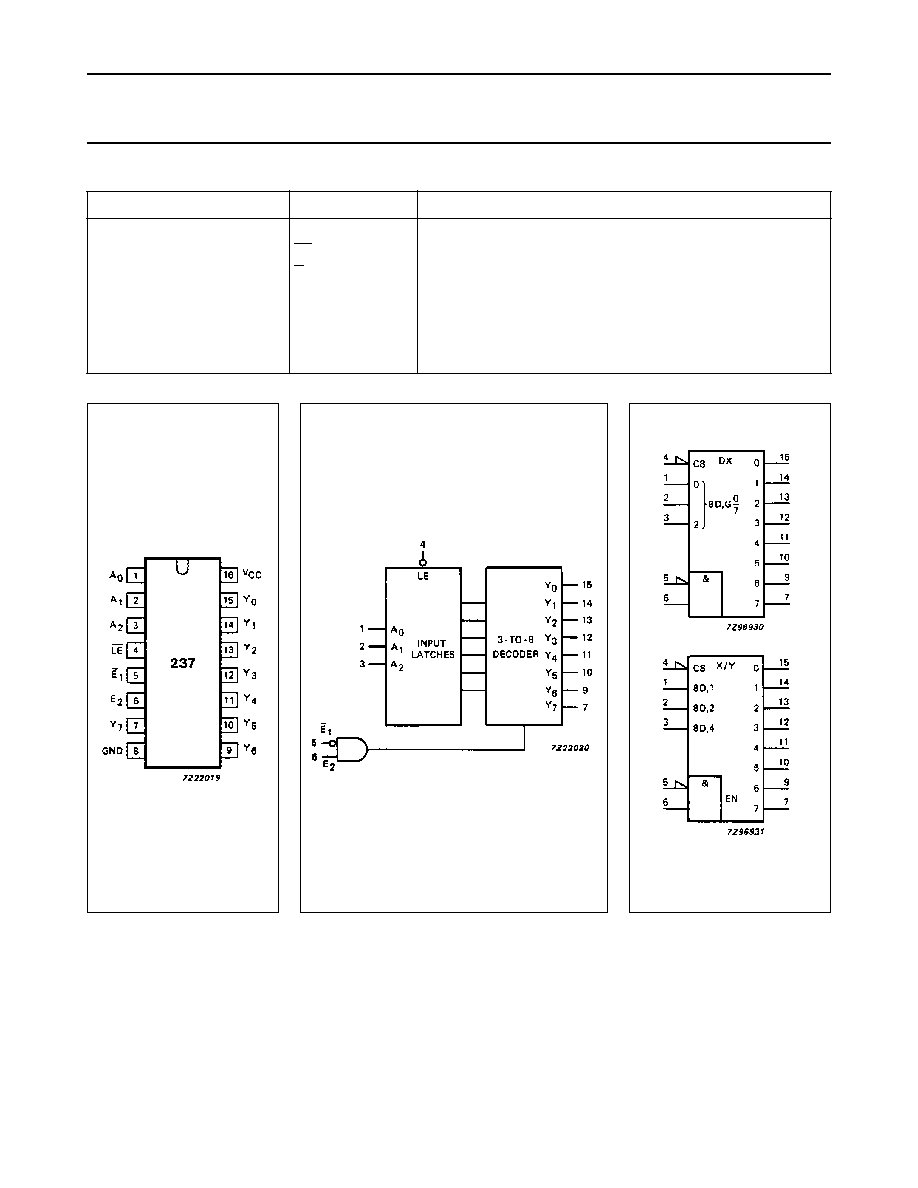
PIN DESCRIPTION
PIN NO.
SYMBOL
NAME AND FUNCTION
1, 2, 3
A
0
to A
2
data inputs
4
LE
latch enable input (active LOW)
5
E
1
data enable input (active LOW)
6
E
2
data enable input (active HIGH)
8
GND
ground (0 V)
15, 14, 13, 12, 11, 10, 9, 7
Y
0
to Y
7
multiplexer outputs
16
V
CC
positive supply voltage
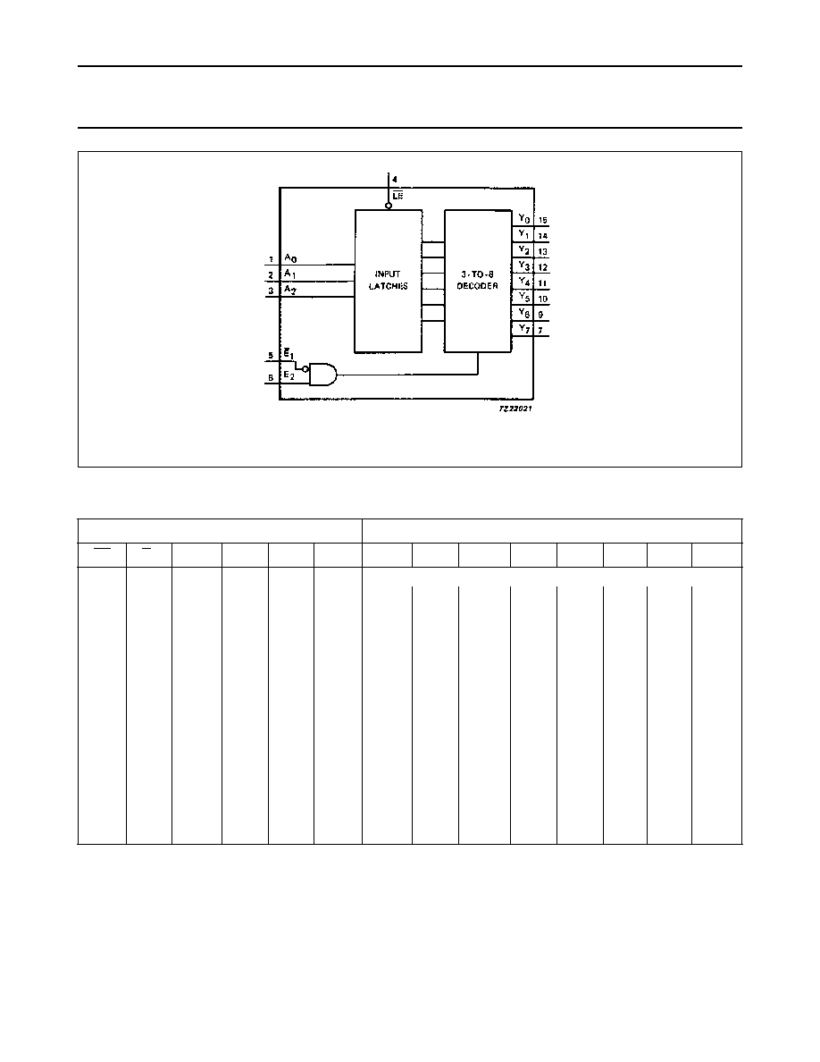
Fig.1 Pin configuration.
Fig.2 Logic symbol.
Fig.3 IEC logic symbol.
December 1990
4
Philips Semiconductors
Product specification
3-to-8 line decoder/demultiplexer with
address latches
74HC/HCT237
FUNCTION TABLE
Notes
1. H = HIGH voltage level
L = LOW voltage level
X = don't care
INPUTS
OUTPUTS
LE
E
1
E
2
A
0
A
1
A
2
Y
0
Y
1
Y
2
Y
3
Y
4
Y
5
Y
6
Y
7
H
L
H
X
X
X
stable
X
H
X
X
X
X
L
L
L
L
L
L
L
L
X
X
L
X
X
X
L
L
L
L
L
L
L
L
L
L
H
L
L
L
H
L
L
L
L
L
L
L
L
L
H
H
L
L
L
H
L
L
L
L
L
L
L
L
H
L
H
L
L
L
H
L
L
L
L
L
L
L
H
H
H
L
L
L
L
H
L
L
L
L
L
L
H
L
L
H
L
L
L
L
H
L
L
L
L
L
H
H
L
H
L
L
L
L
L
H
L
L
L
L
H
L
H
H
L
L
L
L
L
L
H
L
L
L
H
H
H
H
L
L
L
L
L
L
L
H
Fig.4 Functional diagram.