
1.
General description
The 74LVT162374 is a high performance BiCMOS product designed for V
CC
operation at
3.3 V.
The 74LVT162374 is designed with 30
series resistance in both the HIGH and LOW
states of the output. This design reduces line noise in applications such as memory
address drivers, clock drivers, and bus receivers/transmitters.
This device is a 16-bit edge-triggered D-type flip-flop featuring non-inverting 3-state
outputs. The device can be used as two 8-bit flip-flops or one 16-bit flip-flop. On the
positive transition of the clock (CP), the Q outputs of the flip-flop take on the logic levels
set up at the D inputs.
2.
Features
s
16-bit edge-triggered flip-flop
s
3-state buffers
s
Output capability: +12 mA and
-
12 mA
s
TTL input and output switching levels
s
Input and output interface capability to systems at 5 V supply
s
Bus-hold data inputs eliminate the need for external pull-up resistors to hold unused
inputs
s
Live insertion and extraction permitted
s
Outputs include series resistance of 30
making external resistors unnecessary
s
Power-up reset
s
Power-up 3-state
s
No bus current loading when output is tied to 5 V bus
s
Latch-up protection exceeds 500 mA per JESD78
s
ESD protection:
x
MIL STD 883 method 3015: exceeds 2000 V
x
Machine model: exceeds 200 V
74LVT162374
3.3 V 16-bit edge-triggered D-type flip-flop with 30
termination resistors; 3-state
Rev. 03 -- 17 January 2005
Product data sheet
9397 750 14401
© Koninklijke Philips Electronics N.V. 2005. All rights reserved.
Product data sheet
Rev. 03 -- 17 January 2005
2 of 17
Philips Semiconductors
74LVT162374
3.3 V 16-bit edge-triggered D-type flip-flop
3.
Quick reference data
4.
Ordering information
Table 1:
Quick reference data
T
amb
= 25
°
C.
Symbol
Parameter
Conditions
Min
Typ
Max
Unit
t
PLH
, t
PHL
propagation delay
nCP to nQn
C
L
= 50 pF; V
CC
= 3.3 V
-
3.0
-
ns
C
I
input capacitance
V
I
= 0 V or 3.0 V
-
3
-
pF
C
O
output capacitance
outputs disabled;
V
O
= 0 V or 3.0 V
-
9
-
pF
I
CC
supply current
outputs disabled;
V
CC
= 3.6 V
-
70
-
µ
A
Table 2:
Ordering information
Type number
Package
Temperature range
Name
Description
Version
74LVT162374DGG
-
40
°
C to +85
°
C
TSSOP48
plastic thin shrink small outline package;
48 leads; body width 6.1 mm
SOT362-1
74LVT162374DL
-
40
°
C to +85
°
C
SSOP48
plastic shrink small outline package; 48 leads;
body width 7.5 mm
SOT370-1
9397 750 14401
© Koninklijke Philips Electronics N.V. 2005. All rights reserved.
Product data sheet
Rev. 03 -- 17 January 2005
3 of 17
Philips Semiconductors
74LVT162374
3.3 V 16-bit edge-triggered D-type flip-flop
5.
Functional diagram
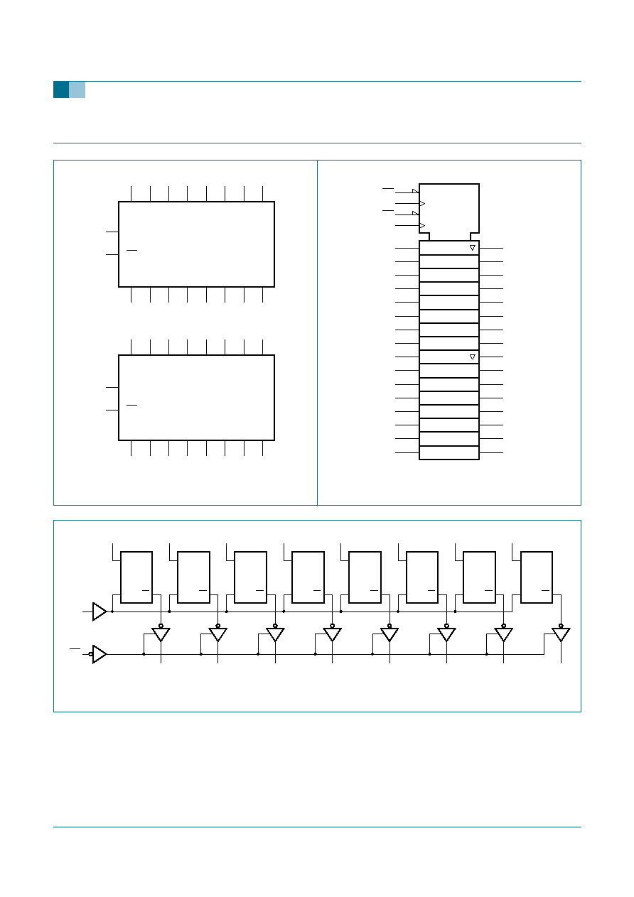
Fig 1.
Logic symbol
Fig 2.
IEC logic symbol
001aac369
1CP
1OE
48
47
1D0
46
1D1
44
1D2
43
1D3
41
1D4
40
1D5
38
1D6
37
2
3
5
6
8
9
11
12
1D7
1Q0 1Q1 1Q2 1Q3 1Q4 1Q5 1Q6 1Q7
1
2CP
2OE
25
36
2D0
35
2D1
33
2D2
32
2D3
30
2D4
29
2D5
27
2D6
26
13
14
16
17
19
20
22
23
2D7
2Q0 2Q1 2Q2 2Q3 2Q4 2Q5 2Q6 2Q7
24
23
001aaa254
37
12
11
9
8
6
5
47
46
44
43
41
40
38
1D7
1D0
1D1
1D2
1D3
1D4
1D5
1D6
2
3
1Q7
1Q6
1Q5
1Q4
1Q3
1Q2
1Q0
1Q1
26
22
20
19
17
16
36
35
33
32
30
29
27
2D5
2D0
2D1
2D2
2D3
2D4
13
14
2Q5
2Q4
2Q3
2Q2
2Q1
2Q0
24
25
2EN
1OE
1
1EN
1CP
2OE
2CP
48
C3
C4
3D
1
4D
2D7
2D6
2Q7
2Q6
2
Fig 3.
Logic diagram
001aac371
D
CP
Q
nD0
nCP
nOE
nQ0
D
CP
Q
nD1
nQ1
D
CP
Q
nD2
nQ2
D
CP
Q
nD3
nQ3
D
CP
Q
nD4
nQ4
D
CP
Q
nD5
nQ5
D
CP
Q
nD6
nQ6
D
CP
Q
nD7
nQ7
9397 750 14401
© Koninklijke Philips Electronics N.V. 2005. All rights reserved.
Product data sheet
Rev. 03 -- 17 January 2005
4 of 17
Philips Semiconductors
74LVT162374
3.3 V 16-bit edge-triggered D-type flip-flop
6.
Pinning information
6.1 Pinning
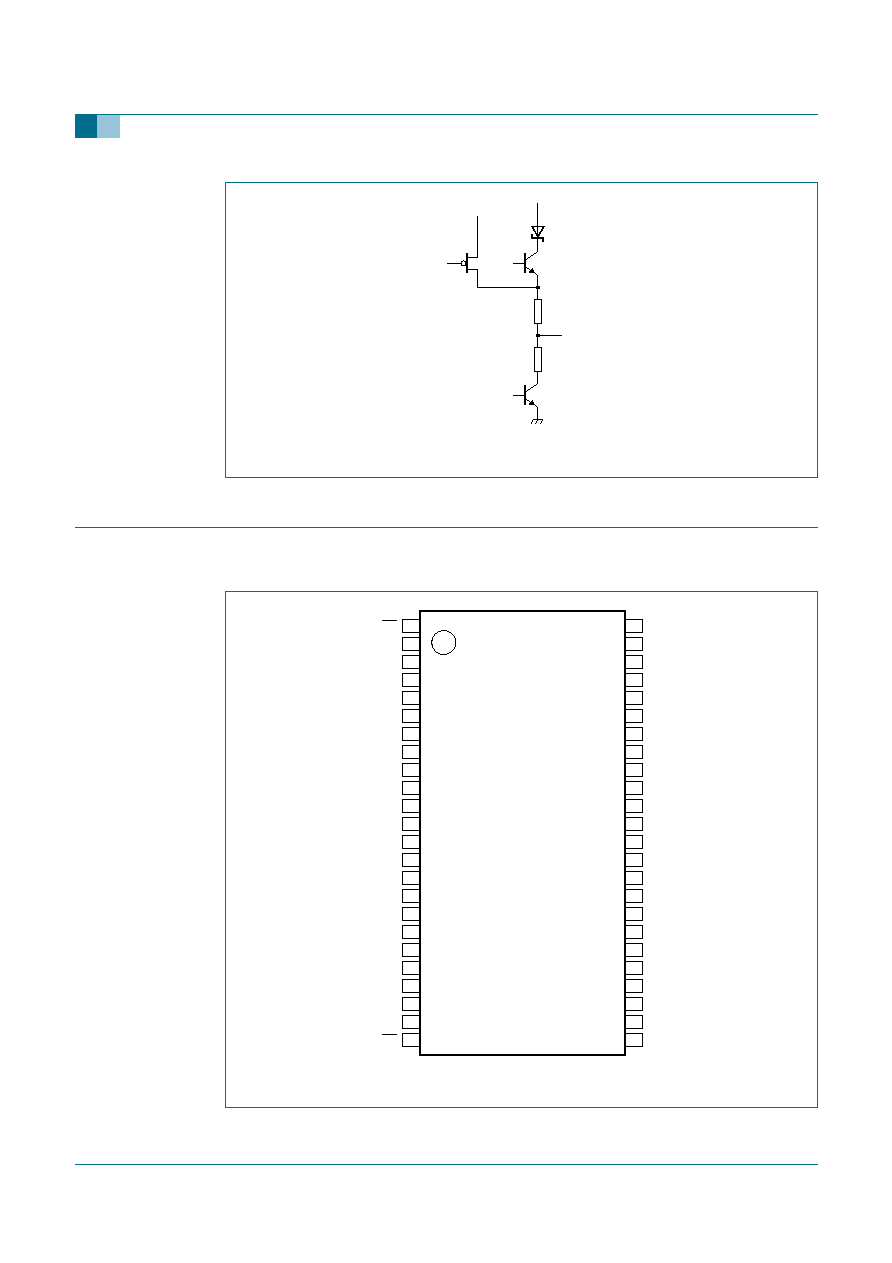
Fig 4.
Output schematic (one output)
001aac372
output
V
CC
27
27
Fig 5.
Pin configuration
162374
001aac370
1
2
3
4
5
6
7
8
9
10
11
12
13
14
15
16
17
18
19
20
21
22
23
24
48
47
46
45
44
43
42
41
40
39
38
37
36
35
34
33
32
31
30
29
28
27
26
25
1Q0
1Q1
GND
1D0
1D1
GND
1OE
1CP
1Q2
1Q3
V
CC
1Q4
1Q5
GND
1Q6
1Q7
2Q0
2Q1
GND
2Q2
2Q3
V
CC
2Q4
2Q5
GND
2Q6
2Q7
2OE
1D2
1D3
V
CC
1D4
1D5
GND
1D6
1D7
2D0
2D1
GND
2D2
2D3
V
CC
2D4
2D5
GND
2D6
2D7
2CP

9397 750 14401
© Koninklijke Philips Electronics N.V. 2005. All rights reserved.
Product data sheet
Rev. 03 -- 17 January 2005
5 of 17
Philips Semiconductors
74LVT162374
3.3 V 16-bit edge-triggered D-type flip-flop
6.2 Pin description
Table 3:
Pin description
Symbol
Pin
Description
1OE
1
output enable input (active LOW)
1Q0
2
data output
1Q1
3
data output
GND
4
ground (0 V)
1Q2
5
data output
1Q3
6
data output
V
CC
7
supply voltage
1Q4
8
data output
1Q5
9
data output
GND
10
ground (0 V)
1Q6
11
data output
1Q7
12
data output
2Q0
13
data output
2Q1
14
data output
GND
15
ground (0 V)
2Q2
16
data output
2Q3
17
data output
V
CC
18
supply voltage
2Q4
19
data output
2Q5
20
data output
GND
21
ground (0 V)
2Q6
22
data output
2Q7
23
data output
2OE
24
output enable input (active LOW)
2CP
25
clock pulse input (active rising edge)
2D7
26
data input
2D6
27
data input
GND
28
ground (0 V)
2D5
29
data input
2D4
30
data input
V
CC
31
supply voltage
2D3
32
data input
2D2
33
data input
GND
34
ground (0 V)
2D1
35
data input
2D0
36
data input
1D7
37
data input
1D6
38
data input
GND
39
ground (0 V)