Äîêóìåíòàöèÿ è îïèñàíèÿ www.docs.chipfind.ru
DATA SHEET
Preliminary specification
2001 Nov 01
DISCRETE SEMICONDUCTORS
BAP1321-01
Silicon PIN diode
M3D319
2001 Nov 01
2
Philips Semiconductors
Preliminary specification
Silicon PIN diode
BAP1321-01
FEATURES
·
High voltage, current controlled
·
RF resistor for RF attenuators and switches
·
Low diode capacitance
·
Low diode forward resistance
·
Very low series inductance
·
For applications up to 3 GHz.
APPLICATIONS
·
RF attenuators and switches.
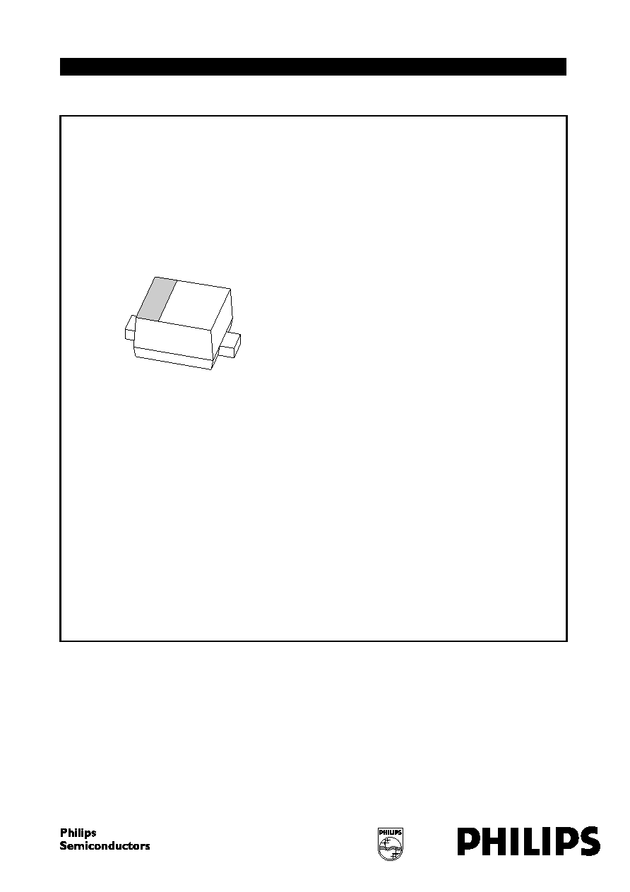
DESCRIPTION
Planar PIN diode in a SOD723A ultra small plastic SMD
package.
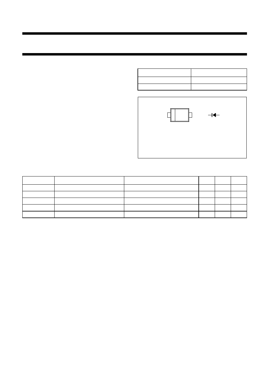
PINNING
PIN
DESCRIPTION
1
cathode
2
anode
handbook, halfpage
1
2
;
Top view
MAM405
Marking code: K7
Fig.1 Simplified outline (SOD723A) and symbol.
LIMITING VALUES
In accordance with the Absolute Maximum Rating System (IEC 60134).
SYMBOL
PARAMETER
CONDITIONS
MIN.
MAX.
UNIT
V
R
continuous reverse voltage
-
60
V
I
F
continuous forward current
-
100
mA
P
tot
total power dissipation
T
s
= 90
°
C
-
315
mW
T
stg
storage temperature
-
65
+150
°
C
T
j
junction temperature
-
65
+150
°
C
2001 Nov 01
3
Philips Semiconductors
Preliminary specification
Silicon PIN diode
BAP1321-01
ELECTRICAL CHARACTERISTICS
T
j
= 25
°
C unless otherwise specified.
Note
1.
Guaranteed on AQL basis: inspection level S4, AQL 1.0.
THERMAL CHARACTERISTICS
SYMBOL
PARAMETER
CONDITIONS
TYP.
MAX.
UNIT
V
F
forward voltage
I
F
= 50 mA
0.95
1.1
V
I
R
reverse leakage current
V
R
= 60 V
-
0.1
µ
A
V
R
= 20 V
-
tbd
µ
A
C
d
diode capacitance
V
R
= 0; f = 1 MHz
0.32
-
pF
V
R
= 1 V; f = 1 MHz
0.28
-
pF
V
R
= 20 V; f = 1 MHz
0.22
0.32
pF
r
D
diode forward resistance
f = 100 MHz; note 1
I
F
= 0.5 mA
3.2
5.0
I
F
= 1 mA
2.3
3.6
I
F
= 10 mA
1.1
1.8
I
F
= 100 mA
0.8
1.3
|
s
21
|
2
isolation
V
R
= 0; f = 900 MHz
15.7
-
dB
V
R
= 0; f = 1800 MHz
10.8
-
dB
V
R
= 0; f = 2450 MHz
8.7
-
dB
|
s
21
|
2
insertion loss
I
F
= 0.5 mA; f = 900 MHz
0.26
-
dB
I
F
= 0.5 mA; f = 1800 MHz
0.28
-
dB
I
F
= 0.5 mA; f = 2450 MHz
0.31
-
dB
|
s
21
|
2
insertion loss
I
F
= 1 mA; f = 900 MHz
0.20
-
dB
I
F
= 1 mA; f = 1800 MHz
0.23
-
dB
I
F
= 1 mA; f = 2450 MHz
0.25
-
dB
|
s
21
|
2
insertion loss
I
F
= 10 mA; f = 900 MHz
0.15
-
dB
I
F
= 10 mA; f = 1800 MHz
0.18
-
dB
I
F
= 10 mA; f = 2450 MHz
0.21
-
dB
|
s
21
|
2
insertion loss
I
F
= 100 mA; f = 900 MHz
0.10
-
dB
I
F
= 100 mA; f = 1800 MHz
0.13
-
dB
I
F
= 100 mA; f = 2450 MHz
0.16
-
dB
L
charge carrier life time
when switched from I
F
= 10 mA to
I
R
= 6 mA; R
L
= 100
;
measured at I
R
= 3 mA
0.5
-
µ
s
L
S
series inductance
I
F
= 100 mA; f = 100 MHz
0.6
-
nH
SYMBOL
PARAMETER
VALUE
UNIT
R
th j-s
thermal resistance from junction to soldering point
190
K/W
2001 Nov 01
4
Philips Semiconductors
Preliminary specification
Silicon PIN diode
BAP1321-01
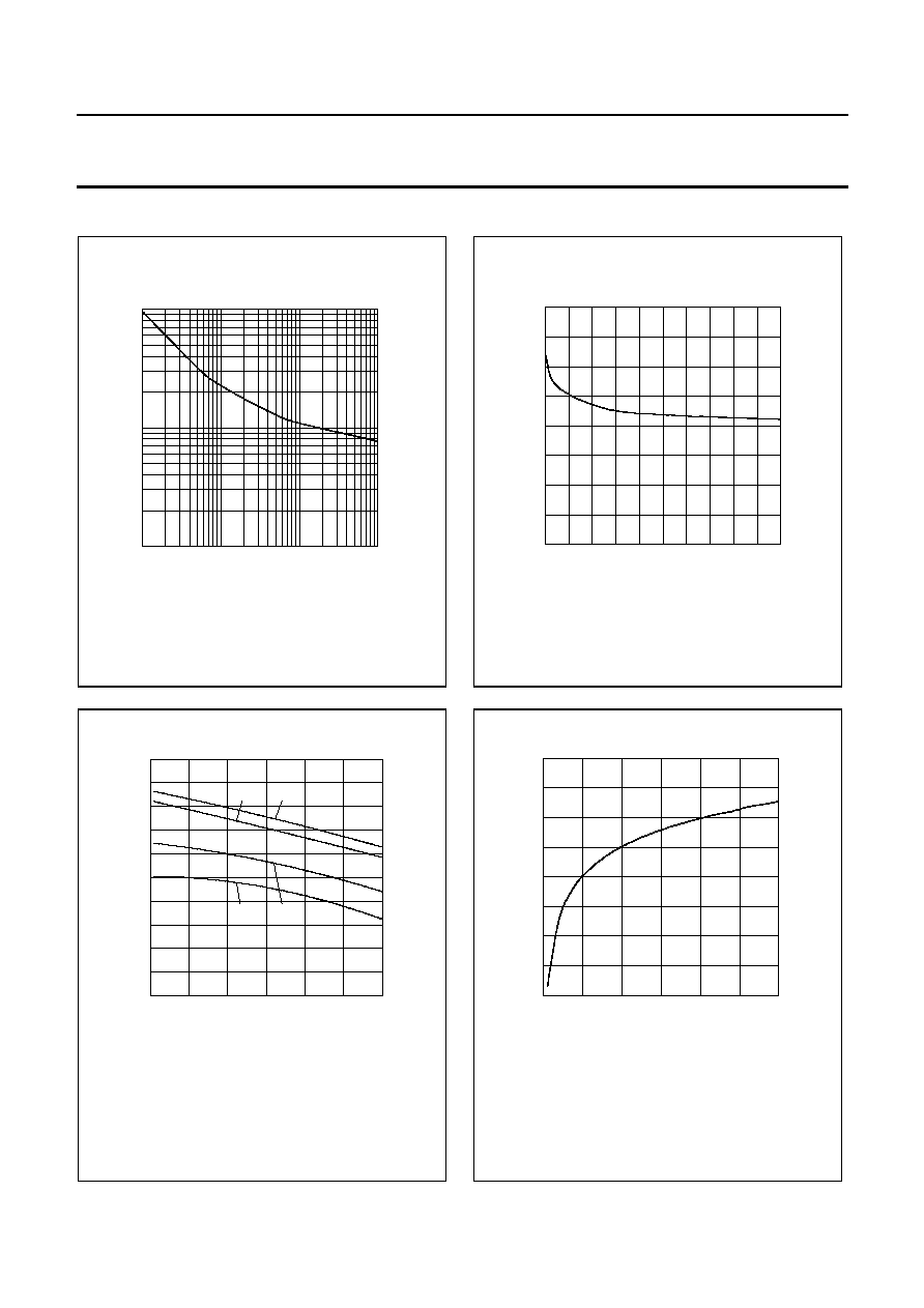
GRAPHICAL DATA
0.1
1
10
0.1
1
10
100
I
F
(mA)
r
D
(
)
Fig.2
Forward resistance as a function of forward
current; typical values.
f = 100 MHz; T
j
= 25
°
C.
0
100
200
300
400
0
4
8
12
16
20
V
R
(V)
C
d
(pF)
f = 1 MHz; T
j
= 25
°
C.
Fig.3
Diode capacitance as a function of reverse
voltage; typical values.
-0.5
-0.4
-0.3
-0.2
-0.1
0
0
1
2
3
f (GHz)
|s
21
|
2
(dB)
(3)
(2)
(1)
(4)
Fig.4
Insertion loss (
|
s
21
|
2
) of the diode as a
function of frequency; typical values.
Diode inserted in series with a 50
stripline circuit and biased
via the analyzer Tee network. T
amb
= 25
°
C.
(1) I
F
= 0.5 mA.
(2) I
F
= 1 mA.
(3) I
F
= 10 mA.
(4) I
F
= 100 mA.
-40
-30
-20
-10
0
0
1
2
3
f (GHz)
|s
21
|
2
(dB)
Fig.5
Isolation (
|
s
21
|
2
) of the diode as a function of
frequency; typical values.
Diode zero biased and inserted in series with a 50
stripline circuit.
T
amb
= 25
°
C.
2001 Nov 01
5
Philips Semiconductors
Preliminary specification
Silicon PIN diode
BAP1321-01
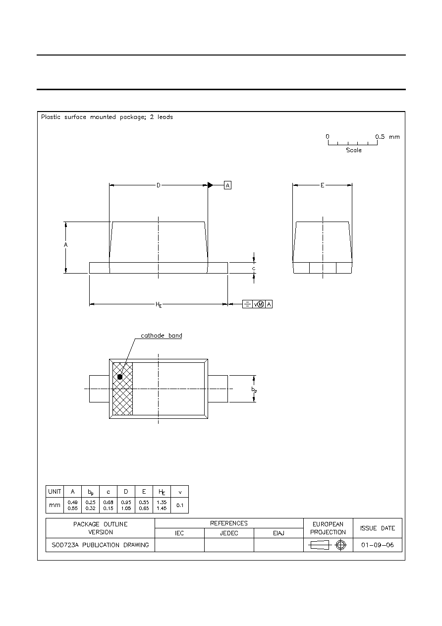
PACKAGE OUTLINE
SOD723A
Fig.6
UNDE
R DEV
ELOP
MENT
Document Outline
- FEATURES
- APPLICATIONS
- DESCRIPTION
- LIMITING VALUES
- PINNING
- ELECTRICAL CHARACTERISTICS
- THERMAL CHARACTERISTICS
- GRAPHICAL DATA
- PACKAGE OUTLINE
- DATA SHEET STATUS
- DEFINITIONS
- DISCLAIMERS