 | –≠–ª–µ–∫—Ç—Ä–æ–Ω–Ω—ã–π –∫–æ–º–ø–æ–Ω–µ–Ω—Ç: BAP50-03 | –°–∫–∞—á–∞—Ç—å:  PDF PDF  ZIP ZIP |

DATA SHEET
Product specification
Supersedes data of 1999 Feb 01
1999 May 10
DISCRETE SEMICONDUCTORS
BAP50-03
General purpose PIN diode
k, halfpage
M3D049

1999 May 10
2
Philips Semiconductors
Product specification
General purpose PIN diode
BAP50-03
FEATURES
∑
Low diode capacitance
∑
Low diode forward resistance.
APPLICATIONS
∑
General RF applications.
DESCRIPTION
General purpose PIN diode in a SOD323 small plastic
SMD package.
PINNING
PIN
DESCRIPTION
1
cathode
2
anode
Fig.1 Simplified outline (SOD323) and symbol.
Marking code: A8.
handbook, halfpage
1
2
MAM406
LIMITING VALUES
In accordance with the Absolute Maximum Rating System (IEC 134).
SYMBOL
PARAMETER
CONDITIONS
MIN.
MAX.
UNIT
V
R
continuous reverse voltage
-
50
V
I
F
continuous forward current
-
50
mA
P
tot
total power dissipation
T
s
= 90
∞
C
-
500
mW
T
stg
storage temperature
-
65
+150
∞
C
T
j
junction temperature
-
65
+150
∞
C

1999 May 10
3
Philips Semiconductors
Product specification
General purpose PIN diode
BAP50-03
ELECTRICAL CHARACTERISTICS
T
j
= 25
∞
C unless otherwise specified.
Note
1. Guaranteed on AQL basis: inspection level S4, AQL 1.0.
THERMAL CHARACTERISTICS
SYMBOL
PARAMETER
CONDITIONS
MIN.
TYP.
MAX.
UNIT
V
F
forward voltage
I
F
= 50 mA
-
0.95
1.1
V
V
R
reverse voltage
I
R
= 10
µ
A
50
-
-
V
I
R
reverse current
V
R
= 50 V
-
-
100
nA
C
d
diode capacitance
V
R
= 0; f = 1 MHz
-
0.4
-
pF
V
R
= 1 V; f = 1 MHz
-
0.3
0.55
pF
V
R
= 5 V; f = 1 MHz
-
0.2
0.35
pF
r
D
diode forward resistance
I
F
= 0.5 mA; f = 100 MHz; note 1
-
25
40
I
F
= 1 mA; f = 100 MHz; note 1
-
14
25
I
F
= 10 mA; f = 100 MHz; note 1
-
3
5
SYMBOL
PARAMETER
VALUE
UNIT
R
th j-s
thermal resistance from junction to soldering point
85
K/W

1999 May 10
4
Philips Semiconductors
Product specification
General purpose PIN diode
BAP50-03
GRAPHICAL DATA
Fig.2
Forward resistance as a function of
forward current; typical values.
f = 100 MHz; T
j
= 25
∞
C.
handbook, halfpage
10
3
10
10
2
1
MGS317
10
-
2
10
-
1
1
10
IF (mA)
r
D
(
)
Fig.3
Diode capacitance as a function of reverse
voltage; typical values.
f = 1 MHz; T
j
= 25
∞
C.
handbook, halfpage
0
20
VR (V)
Cd
(fF)
500
0
100
MGS323
200
300
400
4
8
12
16
Fig.4
Insertion loss (
|
S
21
|
2
) of the diode as a
function of frequency; typical values.
handbook, halfpage
0.5
3
f (GHz)
|
S21
|
2
(dB)
0
-
5
-
4
MGS319
-
3
-
2
-
1
1
(1)
(2)
(3)
1.5
2
2.5
(1) I
F
= 10 mA.
(2) I
F
= 1 mA.
(3) I
F
= 0.5 mA.
Diode inserted in series with a 50
stripline circuit and
biased via the analyzer Tee network.
T
amb
= 25
∞
C.
Fig.5
Isolation (
|
S
21
|
2
) of the diode as a function
of frequency; typical values.
handbook, halfpage
0.5
3
f (GHz)
|
S21
|
2
(dB)
0
-
25
-
20
MGS316
-
15
-
10
-
5
1
1.5
2
2.5
Diode zero biased and inserted in series with a 50
stripline circuit.
T
amb
= 25
∞
C.
1999 May 10
5
Philips Semiconductors
Product specification
General purpose PIN diode
BAP50-03
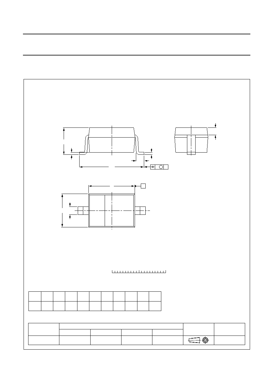
PACKAGE OUTLINE
REFERENCES
OUTLINE
VERSION
EUROPEAN
PROJECTION
ISSUE DATE
IEC
JEDEC
EIAJ
SOD323
98-09-14
0
1
2 mm
scale
SOD323
UNIT
bp
c
D
E
Q
v
mm
0.40
0.25
+
0.05
-
0.05
0.25
0.10
0.2
1.35
1.15
1.8
1.6
A
1.1
0.8
HE
2.7
2.3
0.25
0.15
Lp
0.45
0.15
DIMENSIONS (mm are the original dimensions)
D
1
2
HE
Lp
A
E
bp
A1
Q
Note
1. The marking bar indicates the cathode.
A1
max.
Plastic surface mounted package; 2 leads
,
v
M
A
A
c
(1)