2002 Sep 02
2
Philips Semiconductors
Product specification
Schottky barrier double diode
BAT74V
FEATURES
·
Low forward voltage
·
Low capacitance
·
Ultra small SMD plastic package
·
Flat leads: excellent coplanarity and improved thermal
behaviour.
APPLICATIONS
·
Ultra high-speed switching
·
Voltage clamping
·
Line termination
·
Inverse polarity protection.
DESCRIPTION
Planar Schottky barrier double diode with an integrated
guard ring for stress protection.
Two separate dies encapsulated in a SOT666 ultra small
SMD plastic package.
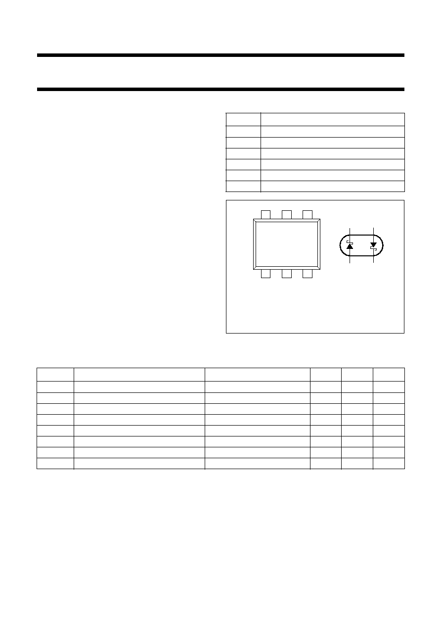
PINNING
PIN
DESCRIPTION
1
anode 1
2
not connected
3
cathode 2
4
anode 2
5
not connected
6
cathode 1
handbook, halfpage
1
2
3
4
6
5
Top view
MAM461
6
4
3
1
Fig.1 Simplified outline (SOT666) and symbol.
Marking code: 74.
LIMITING VALUES
In accordance with the Absolute Maximum Rating System (IEC 60134).
SYMBOL
PARAMETER
CONDITIONS
MIN.
MAX.
UNIT
V
R
continuous reverse voltage
-
30
V
I
F
continuous forward current
-
200
mA
I
FRM
repetitive peak forward current
t
p
1 s;
0.5
-
300
mA
I
FSM
non-repetitive peak forward current
t
p
<
10 ms
600
mA
P
tot
total power dissipation
T
amb
25
°
C
-
230
mW
T
stg
storage temperature
-
65
+150
°
C
T
j
junction temperature
-
125
°
C
T
amb
operating ambient temperature
-
65
+125
°
C
2002 Sep 02
3
Philips Semiconductors
Product specification
Schottky barrier double diode
BAT74V
CHARACTERISTICS
T
amb
= 25
°
C unless otherwise specified.
Note
1. Pulse test: t
p
= 300
µ
s;
= 0.02.
THERMAL CHARACTERISTICS
Note
1. Refer to SOT666 standard mounting conditions.
Soldering
The only recommended soldering method is reflow soldering.
SYMBOL
PARAMETER
CONDITIONS
MAX.
UNIT
V
F
continuous forward voltage
I
F
= 0.1 mA
240
mV
I
F
= 1 mA
320
mV
I
F
= 10 mA
400
mV
I
F
= 30 mA
500
mV
I
F
= 100 mA; note 1; see Fig.2
800
mV
I
R
reverse current
V
R
= 25 V; note 1; see Fig.3
2
µ
A
C
d
diode capacitance
V
R
= 1 V; f = 1 MHz; see Fig.4
10
pF
SYMBOL
PARAMETER
CONDITIONS
VALUE
UNIT
R
th j-a
thermal resistance from junction to ambient
note 1
416
K/W
2002 Sep 02
4
Philips Semiconductors
Product specification
Schottky barrier double diode
BAT74V
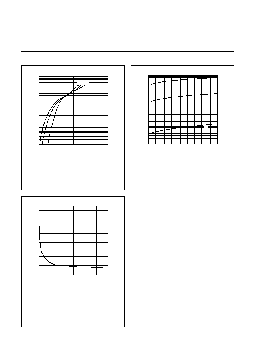
GRAPHICAL DATA
handbook, halfpage
10
IF
VF (V)
3
10
(mA)
2
10
1
10
1
1.2
0.8
0.4
0
MSA892
(3)
(2)
(1)
(3)
(2)
(1)
Fig.2
Forward current as a function of forward
voltage; typical values.
(1) T
amb
= 125
°
C.
(2) T
amb
= 85
°
C.
(3) T
amb
= 25
°
C.
0
10
20
30
V (V)
R
10
3
I
R
(
µ
A)
10
2
10
1
10
1
(1)
(2)
(3)
MSA893
Fig.3
Reverse current as a function of reverse
voltage; typical values.
(1) T
amb
= 125
°
C.
(2) T
amb
= 85
°
C.
(3) T
amb
= 25
°
C.
handbook, halfpage
0
10
20
30
0
5
10
15
VR (V)
Cd
(pF)
MSA891
Fig.4
Diode capacitance as a function of reverse
voltage; typical values.
f = 1 MHz; T
amb
= 25
°
C.
2002 Sep 02
5
Philips Semiconductors
Product specification
Schottky barrier double diode
BAT74V
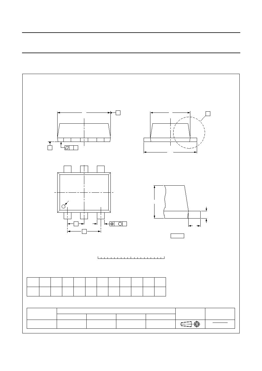
PACKAGE OUTLINE
UNIT
b
p
c
D
E
e
1
H
E
L
p
w
REFERENCES
OUTLINE
VERSION
EUROPEAN
PROJECTION
ISSUE DATE
01-01-04
01-08-27
IEC
JEDEC
EIAJ
mm
0.27
0.17
0.18
0.08
1.7
1.5
1.3
1.1
0.5
e
1.0
1.7
1.5
0.1
y
0.1
DIMENSIONS (mm are the original dimensions)
0.3
0.1
SOT666
bp
pin 1 index
D
e1
e
A
Lp
detail X
HE
E
A
S
0
1
2 mm
scale
A
0.6
0.5
c
X
1
2
3
4
5
6
Plastic surface mounted package; 6 leads
SOT666
Y S
w
M
A