 | –≠–ª–µ–∫—Ç—Ä–æ–Ω–Ω—ã–π –∫–æ–º–ø–æ–Ω–µ–Ω—Ç: BD138-10 | –°–∫–∞—á–∞—Ç—å:  PDF PDF  ZIP ZIP |

DATA SHEET
Product specification
Supersedes data of 1997 Mar 26
1999 Apr 12
DISCRETE SEMICONDUCTORS
BD136; BD138; BD140
PNP power transistors
ok, halfpage
M3D100
1999 Apr 12
2
Philips Semiconductors
Product specification
PNP power transistors
BD136; BD138; BD140
FEATURES
∑
High current (max. 1.5 A)
∑
Low voltage (max. 80 V).
APPLICATIONS
∑
General purpose power applications, e.g. driver stages
in hi-fi amplifiers and television circuits.
DESCRIPTION
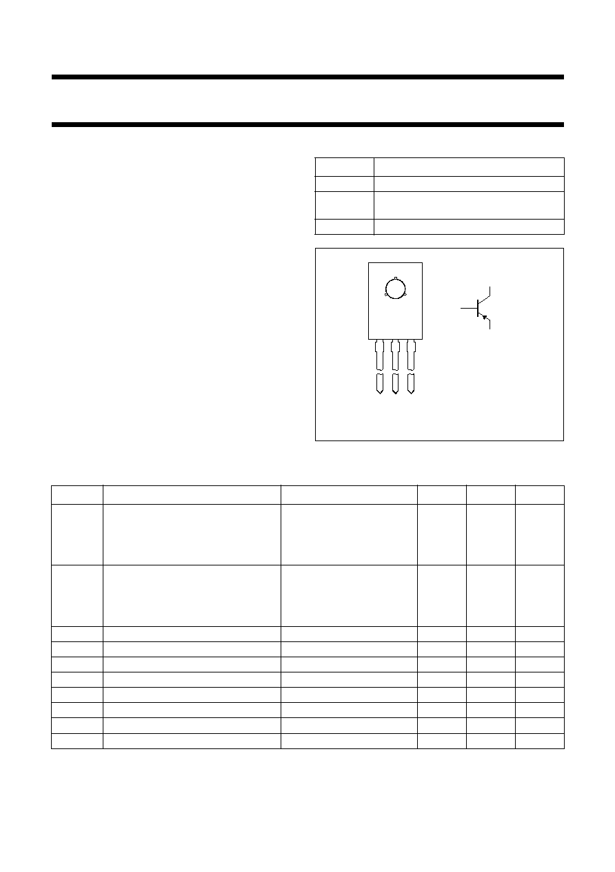
PNP power transistor in a TO-126; SOT32 plastic
package. NPN complements: BD135, BD137 and BD139.
PINNING
PIN
DESCRIPTION
1
emitter
2
collector, connected to metal part of
mounting surface
3
base
Fig.1
Simplified outline (TO-126; SOT32)
and symbol.
handbook, halfpage
MAM272
1
2
3
Top view
1
2
3
LIMITING VALUES
In accordance with the Absolute Maximum Rating System (IEC 134).
SYMBOL
PARAMETER
CONDITIONS
MIN.
MAX.
UNIT
V
CBO
collector-base voltage
open emitter
BD136
-
-
45
V
BD138
-
-
60
V
BD140
-
-
100
V
V
CEO
collector-emitter voltage
open base
BD136
-
-
45
V
BD138
-
-
60
V
BD140
-
-
80
V
V
EBO
emitter-base voltage
open collector
-
-
5
V
I
C
collector current (DC)
-
-
1.5
A
I
CM
peak collector current
-
-
2
A
I
BM
peak base current
-
-
1
A
P
tot
total power dissipation
T
mb
70
∞
C
-
8
W
T
stg
storage temperature
-
65
+150
∞
C
T
j
junction temperature
-
150
∞
C
T
amb
operating ambient temperature
-
65
+150
∞
C

1999 Apr 12
3
Philips Semiconductors
Product specification
PNP power transistors
BD136; BD138; BD140
THERMAL CHARACTERISTICS
Note
1. Refer to TO-126 (SOT32) standard mounting conditions.
CHARACTERISTICS
T
j
= 25
∞
C unless otherwise specified.
SYMBOL
PARAMETER
CONDITIONS
VALUE
UNIT
R
th j-a
thermal resistance from junction to ambient
note 1
100
K/W
R
th j-mb
thermal resistance from junction to mounting base
10
K/W
SYMBOL
PARAMETER
CONDITIONS
MIN.
TYP.
MAX.
UNIT
I
CBO
collector cut-off current
I
E
= 0; V
CB
=
-
30 V
-
-
-
100
nA
I
E
= 0; V
CB
=
-
30 V; T
j
= 125
∞
C
-
-
-
10
µ
A
I
EBO
emitter cut-off current
I
C
= 0; V
EB
=
-
5 V
-
-
-
100
nA
h
FE
DC current gain
V
CE
=
-
2 V; (see Fig.2)
I
C
=
-
5 mA
40
-
-
I
C
=
-
150 mA
63
-
250
I
C
=
-
500 mA
25
-
-
DC current gain
I
C
=
-
150 mA; V
CE
=
-
2 V;
(see Fig.2)
BD136-10; BD138-10; BD140-10
63
-
160
BD136-16; BD138-16; BD140-16
100
-
250
V
CEsat
collector-emitter saturation voltage
I
C
=
-
500 mA; I
B
=
-
50 mA
-
-
-
0.5
V
V
BE
base-emitter voltage
I
C
=
-
500 mA; V
CE
=
-
2 V
-
-
-
1
V
f
T
transition frequency
I
C
=
-
50 mA; V
CE
=
-
5 V;
f = 100 MHz
-
160
-
MHz
DC current gain ratio of the
complementary pairs
I
C
= 150 mA;
V
CE
= 2 V
-
1.3
1.6
h
FE1
h
FE2
-----------
1999 Apr 12
4
Philips Semiconductors
Product specification
PNP power transistors
BD136; BD138; BD140
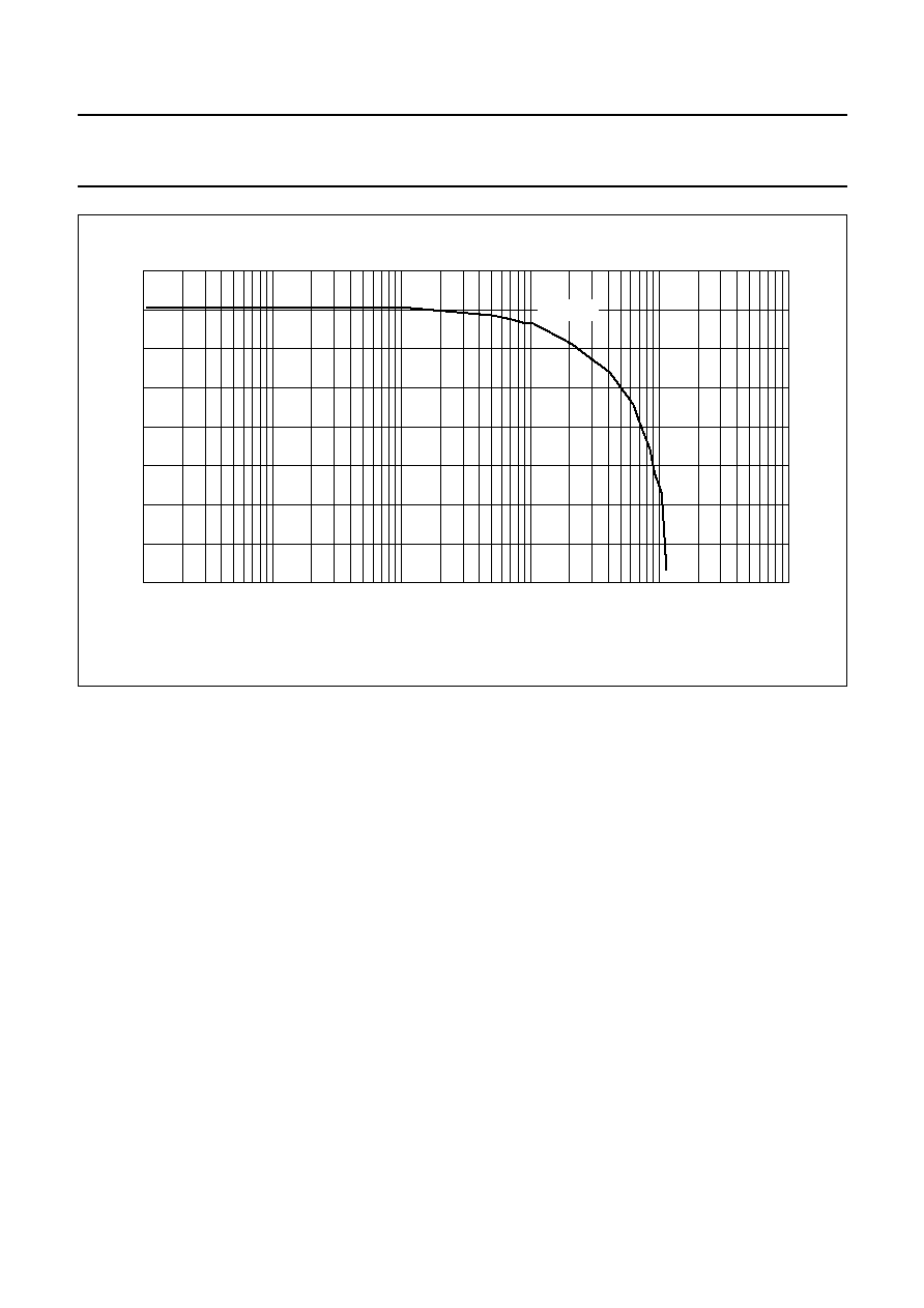
Fig.2 DC current gain; typical values.
handbook, full pagewidth
0
160
80
120
40
MBH730
-
10
-
1
hFE
-
1
IC (mA)
-
10
-
10
3
-
10
4
-
10
2
VCE =
-
2 V

1999 Apr 12
5
Philips Semiconductors
Product specification
PNP power transistors
BD136; BD138; BD140
PACKAGE OUTLINE
UNIT
b
p
c
D
E
e1
L
Q
w
REFERENCES
OUTLINE
VERSION
EUROPEAN
PROJECTION
ISSUE DATE
IEC
JEDEC
EIAJ
mm
0.88
0.65
2.7
2.3
0.60
0.45
11.1
10.5
7.8
7.2
2.29
e
4.58
0.254
P
3.2
3.0
P1
3.9
3.6
DIMENSIONS (mm are the original dimensions)
Note
1. Terminal dimensions within this zone are uncontrolled to allow for flow of plastic and terminal irregularities.
16.5
15.3
1.5
0.9
L1
(1)
max
2.54
SOT32
TO-126
97-03-04
0
2.5
5 mm
scale
A
Plastic single-ended leaded (through hole) package; mountable to heatsink, 1 mounting hole; 3 leads
SOT32
D
P1
P
E
e1
A
L
Q
c
bp
1
2
3
L1
w
M
e