 | –≠–ª–µ–∫—Ç—Ä–æ–Ω–Ω—ã–π –∫–æ–º–ø–æ–Ω–µ–Ω—Ç: BF904 | –°–∫–∞—á–∞—Ç—å:  PDF PDF  ZIP ZIP |

DATA SHEET
Product specification
Supersedes data of 1997 Sep 05
1999 May 17
DISCRETE SEMICONDUCTORS
BF904; BF904R
N-channel dual gate MOS-FETs

1999 May 17
2
Philips Semiconductors
Product specification
N-channel dual gate MOS-FETs
BF904; BF904R
FEATURES
∑
Specially designed for use at 5 V supply voltage
∑
Short channel transistor with high transfer admittance to
input capacitance ratio
∑
Low noise gain controlled amplifier up to 1 GHz
∑
Superior cross-modulation performance during AGC.
APPLICATIONS
∑
VHF and UHF applications with 3 to 7 V supply voltage
such as television tuners and professional
communications equipment.
DESCRIPTION
Enhancement type field-effect transistor in a plastic
microminiature SOT143B and SOT143R package. The
transistor consists of an amplifier MOS-FET with source
and substrate interconnected and an internal bias circuit to
ensure good cross-modulation performance during AGC.
PINNING
CAUTION
This product is supplied in anti-static packing to
prevent damage caused by electrostatic discharge
during transport and handling. For further information,
refer to Philips specs.: SNW-EQ-608, SNW-FQ-302A
and SNW-FQ-302B.
PIN
SYMBOL
DESCRIPTION
1
s, b
source
2
d
drain
3
g
2
gate 2
4
g
1
gate 1
Fig.1 Simplified outline (SOT143B) and symbol.
BF904 marking code: M04.
handbook, halfpage
4
3
2
1
Top view
MAM124
s,b
d
g
1
g
2
Fig.2 Simplified outline (SOT143R) and symbol.
BF904R marking code: M06.
handbook, halfpage
Top view
MAM125 - 1
s,b
d
g
1
g
2
3
4
1
2
QUICK REFERENCE DATA
SYMBOL
PARAMETER
CONDITIONS
MIN.
TYP.
MAX.
UNIT
V
DS
drain-source voltage
-
-
7
V
I
D
drain current
-
-
30
mA
P
tot
total power dissipation
-
-
200
mW
T
j
operating junction temperature
-
-
150
∞
C
y
fs
forward transfer admittance
22
25
30
mS
C
ig1-s
input capacitance at gate 1
-
2.2
2.6
pF
C
rs
reverse transfer capacitance
f = 1 MHz
-
25
35
fF
F
noise figure
f = 800 MHz
-
2
-
dB
1999 May 17
3
Philips Semiconductors
Product specification
N-channel dual gate MOS-FETs
BF904; BF904R
LIMITING VALUES
In accordance with the Absolute Maximum Rating System (IEC 134).
Note
1. Device mounted on a printed-circuit board.
SYMBOL
PARAMETER
CONDITIONS
MIN.
MAX.
UNIT
V
DS
drain-source voltage
-
7
V
I
D
drain current
-
30
mA
I
G1
gate 1 current
-
±
10
mA
I
G2
gate 2 current
-
±
10
mA
P
tot
total power dissipation
see Fig.3
BF904
T
amb
50
∞
C; note 1
-
200
mW
BF904R
T
amb
40
∞
C; note 1
-
200
mW
T
stg
storage temperature
-
65
+150
∞
C
T
j
operating junction temperature
-
150
∞
C
Fig.3 Power derating curves.
handbook, halfpage
0
50
100
150
200
250
0
50
100
150
200
P
tot
(mW)
MRA770
Tamb ( C)
o
BF904
BF904R

1999 May 17
4
Philips Semiconductors
Product specification
N-channel dual gate MOS-FETs
BF904; BF904R
THERMAL CHARACTERISTICS
Notes
1. Device mounted on a printed-circuit board.
2. T
s
is the temperature at the soldering point of the source lead.
STATIC CHARACTERISTICS
T
j
= 25
∞
C unless otherwise specified.
Note
1. R
G1
connects gate 1 to V
GG
= 5 V; see Fig.20.
DYNAMIC CHARACTERISTICS
Common source; T
amb
= 25
∞
C; V
DS
= 5 V; V
G2-S
= 4 V; I
D
= 10 mA; unless otherwise specified.
SYMBOL
PARAMETER
CONDITIONS
VALUE
UNIT
R
th j-a
thermal resistance from junction to ambient
note 1
BF904
500
K/W
BF904R
550
K/W
R
th j-s
thermal resistance from junction to soldering point
note 2
BF904
T
s
= 92
∞
C
290
K/W
BF904R
T
s
= 78
∞
C
360
K/W
SYMBOL
PARAMETER
CONDITIONS
MIN.
MAX.
UNIT
V
(BR)G1-SS
gate 1-source breakdown voltage
V
G2-S
= V
DS
= 0; I
G1-S
= 10 mA
6
15
V
V
(BR)G2-SS
gate 2-source breakdown voltage
V
G1-S
= V
DS
= 0; I
G2-S
= 10 mA
6
15
V
V
(F)S-G1
forward source-gate 1 voltage
V
G2-S
= V
DS
= 0; I
S-G1
= 10 mA
0.5
1.5
V
V
(F)S-G2
forward source-gate 2 voltage
V
G1-S
= V
DS
= 0; I
S-G2
= 10 mA
0.5
1.5
V
V
G1-S(th)
gate 1-source threshold voltage
V
G2-S
= 4 V; V
DS
= 5 V; I
D
= 20
µ
A
0.3
1
V
V
G2-S(th)
gate 2-source threshold voltage
V
G1-S
= V
DS
= 5 V; I
D
= 20
µ
A
0.3
1.2
V
I
DSX
drain-source current
V
G2-S
= 4 V; V
DS
= 5 V;
R
G1
= 120 k
; note 1
8
13
mA
I
G1-SS
gate 1 cut-off current
V
G2-S
= V
DS
= 0; V
G1-S
= 5 V
-
50
nA
I
G2-SS
gate 2 cut-off current
V
G1-S
= V
DS
= 0; V
G2-S
= 5 V
-
50
nA
SYMBOL
PARAMETER
CONDITIONS
MIN.
TYP.
MAX.
UNIT
y
fs
forward transfer admittance
pulsed; T
j
= 25
∞
C
22
25
30
mS
C
ig1-s
input capacitance at gate 1
f = 1 MHz
-
2.2
2.6
pF
C
ig2-s
input capacitance at gate 2
f = 1 MHz
1
1.5
2
pF
C
os
drain-source capacitance
f = 1 MHz
1
1.3
1.6
pF
C
rs
reverse transfer capacitance f = 1 MHz
-
25
35
fF
F
noise figure
f = 200 MHz; G
S
= 2 mS; B
S
= B
Sopt
-
1
1.5
dB
f = 800 MHz; G
S
= G
Sopt
; B
S
= B
Sopt
-
2
2.8
dB
1999 May 17
5
Philips Semiconductors
Product specification
N-channel dual gate MOS-FETs
BF904; BF904R
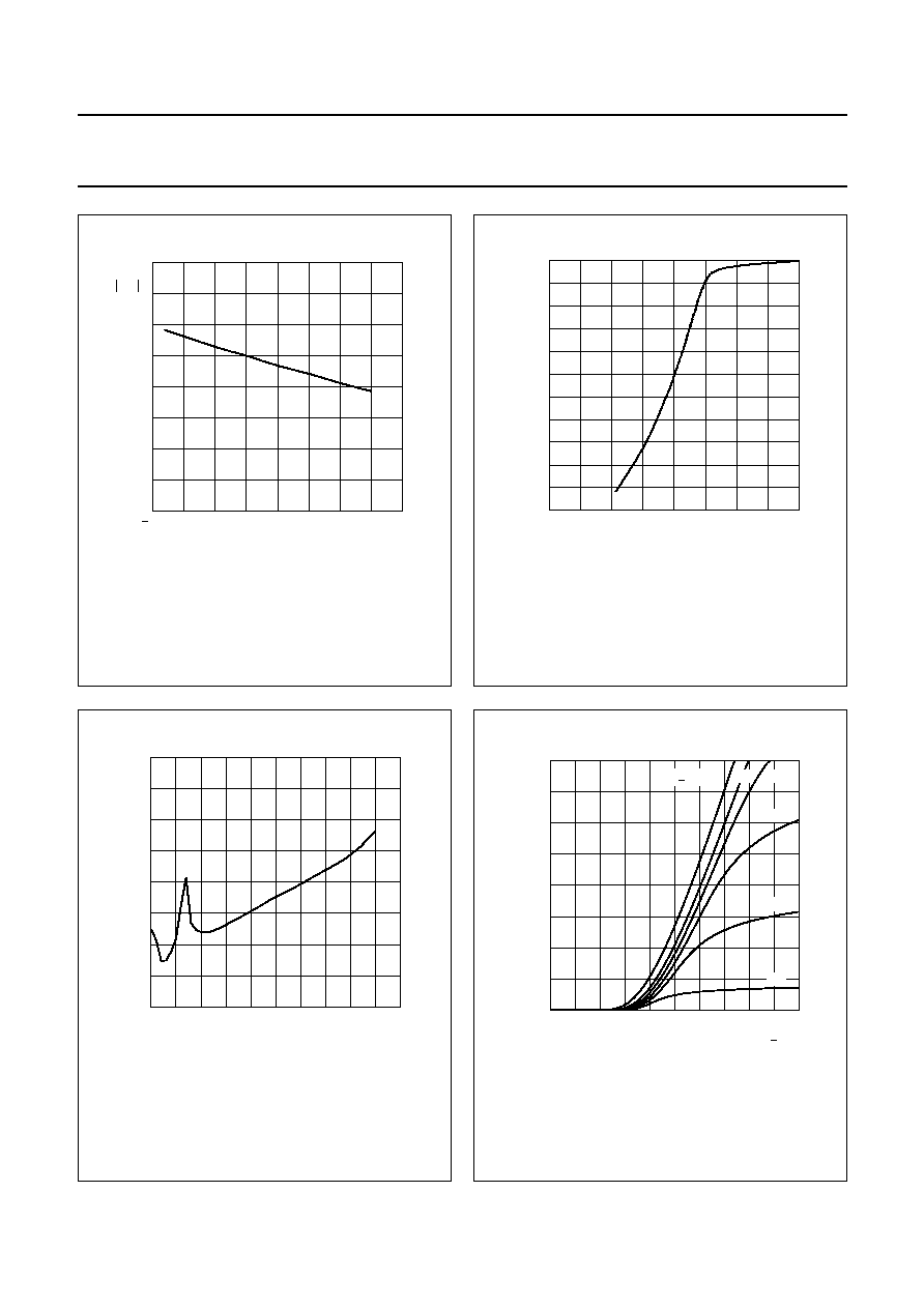
Fig.4
Transfer admittance as a function of the
junction temperature; typical values.
50
0
50
150
30
0
MLD268
100
T ( C)
o
j
Yfs
(mS)
40
20
10
Fig.5
Typical gain reduction as a function of
the AGC voltage.
f = 50 MHz.
handbook, halfpage
0
10
20
30
40
50
0
1
2
3
4
V (V)
AGC
gain
reduction
(dB)
MRA769
Fig.6
Unwanted voltage for 1% cross-modulation
as a function of gain reduction; typical
values; see Fig.20.
V
DS
= 5 V; V
GG
= 5 V; f
w
= 50 MHz.
f
unw
= 60 MHz; T
amb
= 25
∞
C; R
G1
= 120 k
.
handbook, halfpage
80
90
100
110
120
0
10
20
30
40
50
Vunw
(dB V)
gain reduction (dB)
MRA771
µ
Fig.7 Transfer characteristics; typical values.
V
DS
= 5 V.
T
j
= 25
∞
C.
0
20
10
15
5
0
0.4
2.0
MLD270
0.8
1.2
1.6
I D
(mA)
V (V)
G1 S
2 V
1.5 V
1 V
V = 4 V
3 V
2.5 V
G2 S