 | –≠–ª–µ–∫—Ç—Ä–æ–Ω–Ω—ã–π –∫–æ–º–ø–æ–Ω–µ–Ω—Ç: BF909 | –°–∫–∞—á–∞—Ç—å:  PDF PDF  ZIP ZIP |

DATA SHEET
Product specification
File under Discrete Semiconductors, SC07
1995 Apr 25
DISCRETE SEMICONDUCTORS
Philips Semiconductors
BF909; BF909R
N-channel dual gate MOS-FETs

1995 Apr 25
2
Philips Semiconductors
Product specification
N-channel dual gate MOS-FETs
BF909; BF909R
FEATURES
∑
Specially designed for use at 5 V supply voltage
∑
High forward transfer admittance
∑
Short channel transistor with high forward transfer
admittance to input capacitance ratio
∑
Low noise gain controlled amplifier up to 1 GHz
∑
Superior cross-modulation performance during AGC.
APPLICATIONS
∑
VHF and UHF applications with 3 to 7 V supply voltage
such as television tuners and professional
communications equipment.
DESCRIPTION
Enhancement type field-effect transistor in a plastic
microminiature SOT143 or SOT143R package. The
transistor consists of an amplifier MOS-FET with source
and substrate interconnected and an internal bias circuit to
ensure good cross-modulation performance during AGC.
PINNING
CAUTION
The device is supplied in an antistatic package. The
gate-source input must be protected against static
discharge during transport or handling.
PIN
SYMBOL
DESCRIPTION
1
s, b
source
2
d
drain
3
g
2
gate 2
4
g
1
gate 1
Fig.1 Simplified outline (SOT143) and symbol.
BF909 marking code: M28.
handbook, halfpage
4
3
2
1
Top view
MAM124
s,b
d
g
1
g
2
Fig.2 Simplified outline (SOT143R) and symbol.
BF909R marking code: M29.
handbook, halfpage
Top view
MAM125 - 1
s,b
d
g
1
g
2
3
4
1
2
QUICK REFERENCE DATA
SYMBOL
PARAMETER
CONDITIONS
MIN.
TYP.
MAX.
UNIT
V
DS
drain-source voltage
-
-
7
V
I
D
drain current
-
-
40
mA
P
tot
total power dissipation
-
-
200
mW
T
j
operating junction temperature
-
-
150
∞
C
y
fs
forward transfer admittance
36
43
50
mS
C
ig1-s
input capacitance at gate 1
-
3.6
4.3
pF
C
rs
reverse transfer capacitance
f = 1 MHz
-
35
50
fF
F
noise figure
f = 800 MHz
-
2
2.8
dB

1995 Apr 25
3
Philips Semiconductors
Product specification
N-channel dual gate MOS-FETs
BF909; BF909R
LIMITING VALUES
In accordance with the Absolute Maximum Rating System (IEC 134).
Note
1. Device mounted on a printed-circuit board.
SYMBOL
PARAMETER
CONDITIONS
MIN.
MAX.
UNIT
V
DS
drain-source voltage
-
7
V
I
D
drain current
-
40
mA
I
G1
gate 1 current
-
±
10
mA
I
G2
gate 2 current
-
±
10
mA
P
tot
total power dissipation
see Fig.3
BF909
up to T
amb
= 50
∞
C; note 1
-
200
mW
BF909R
up to T
amb
= 40
∞
C; note 1
-
200
mW
T
stg
storage temperature
-
65
+150
∞
C
T
j
operating junction temperature
-
150
∞
C
Fig.3 Power derating curves.
handbook, halfpage
0
50
100
200
250
0
200
MLB935
150
150
100
50
Ptot
(mW)
T ( C)
amb
o
BF909R
BF909

1995 Apr 25
4
Philips Semiconductors
Product specification
N-channel dual gate MOS-FETs
BF909; BF909R
THERMAL CHARACTERISTICS
Notes
1. Device mounted on a printed-circuit board.
2. T
s
is the temperature at the soldering point of the source lead.
STATIC CHARACTERISTICS
T
j
= 25
∞
C; unless otherwise specified.
Note
1. R
G1
connects gate 1 to V
GG
= 5 V; see Fig.18.
DYNAMIC CHARACTERISTICS
Common source; T
amb
= 25
∞
C; V
DS
= 5 V; V
G2-S
= 4 V; I
D
= 15 mA; unless otherwise specified.
SYMBOL
PARAMETER
CONDITIONS
VALUE
UNIT
R
th j-a
thermal resistance from junction to ambient
note 1
BF909
500
K/W
BF909R
550
K/W
R
th j-s
thermal resistance from junction to soldering point
note 2
BF909
T
s
= 92
∞
C
290
K/W
BF909R
T
s
= 78
∞
C
360
K/W
SYMBOL
PARAMETER
CONDITIONS
MIN.
MAX.
UNIT
V
(BR)G1-SS
gate 1-source breakdown voltage
V
G2-S
= V
DS
= 0; I
G1-S
= 10 mA
6
15
V
V
(BR)G2-SS
gate 2-source breakdown voltage
V
G1-S
= V
DS
= 0; I
G2-S
= 10 mA
6
15
V
V
(F)S-G1
forward source-gate 1 voltage
V
G2-S
= V
DS
= 0; I
S-G1
= 10 mA
0.5
1.5
V
V
(F)S-G2
forward source-gate 2 voltage
V
G1-S
= V
DS
= 0; I
S-G2
= 10 mA
0.5
1.5
V
V
G1-S(th)
gate 1-source threshold voltage
V
G2-S
= 4 V; V
DS
= 5 V;
I
D
= 20
µ
A
0.3
1
V
V
G2-S(th)
gate 2-source threshold voltage
V
G1-S
= V
DS
= 5 V; I
D
= 20
µ
A
0.3
1.2
V
I
DSX
drain-source current
V
G2-S
= 4 V; V
DS
= 5 V;
R
G1
= 120 k
; note 1
12
20
mA
I
G1-SS
gate 1 cut-off current
V
G1-S
= 5 V; V
G2-S
= V
DS
= 0
-
50
nA
I
G2-SS
gate 2 cut-off current
V
G2-S
= 5 V; V
G1-S
= V
DS
= 0
-
50
nA
SYMBOL
PARAMETER
CONDITIONS
MIN.
TYP.
MAX.
UNIT
y
fs
forward transfer admittance
pulsed; T
j
= 25
∞
C
36
43
50
mS
C
ig1-s
input capacitance at gate 1
f = 1 MHz
-
3.6
4.3
pF
C
ig2-s
input capacitance at gate 2
f = 1 MHz
-
2.3
3
pF
C
os
drain-source capacitance
f = 1 MHz
-
2.3
3
pF
C
rs
reverse transfer capacitance f = 1 MHz
-
35
50
fF
F
noise figure
f = 800 MHz; G
S
= G
Sopt
; B
S
= B
Sopt
-
2
2.8
dB

1995 Apr 25
5
Philips Semiconductors
Product specification
N-channel dual gate MOS-FETs
BF909; BF909R
Fig.4
Unwanted voltage for 1% cross-modulation
as a function of gain reduction; typical
values; see Fig.18.
V
DS
= 5 V; V
GG
= 5 V; f
w
= 50 MHz.
f
unw
= 60 MHz; T
amb
= 25
∞
C; R
G1
= 120 k
.
handbook, halfpage
0
110
100
90
80
10
50
MLB936
20
30
40
Vunw
(dB
µ
V)
gain reduction (dB)
Fig.5 Transfer characteristics; typical values.
V
DS
= 5 V.
T
j
= 25
∞
C.
handbook, halfpage
0
30
20
10
0
0.4
2.0
MLB937
0.8
1.2
1.6
I D
(mA)
V (V)
G1 S
V = 4 V 3 V
2.5 V
2 V
1.5 V
1 V
G2 S
Fig.6 Output characteristics; typical values.
V
DS
= 5 V.
V
G2-S
= 4 V.
T
j
= 25
∞
C.
handbook, halfpage
0
30
20
10
0
2
10
MLB938
4
6
8
I D
(mA)
V (V)
DS
1.3 V
1.2 V
1.1 V
1.0 V
0.9 V
V = 1.4 V
G1 S
Fig.7
Gate 1 current as a function of gate 1
voltage; typical values.
V
DS
= 5 V.
T
j
= 25
∞
C.
handbook, halfpage
0
1
2
3
200
150
50
0
100
MLB939
I G1
(
µ
A)
V (V)
G1 S
3 V
2.5 V
2 V
3.5 V
V = 4 V
G2 S

1995 Apr 25
6
Philips Semiconductors
Product specification
N-channel dual gate MOS-FETs
BF909; BF909R
Fig.8
Forward transfer admittance as a
function of drain current; typical values.
V
DS
= 5 V.
T
j
= 25
∞
C.
handbook, halfpage
0
60
40
20
0
10
20
30
MLB940
y fs
(mS)
I (mA)
D
3.5 V
3 V
2.5 V
2 V
V = 4 V
G2 S
Fig.9
Drain current as a function of gate 1 current;
typical values.
V
DS
= 5 V; V
G2-S
= 4 V.
T
j
= 25
∞
C.
handbook, halfpage
0
20
40
60
25
0
20
MLB941
15
10
5
I (
µ
A)
G1
I D
(mA)
Fig.10 Drain current as a function of gate 1
supply voltage (= V
GG
); typical values;
see Fig.18.
V
DS
= 5 V; V
G2-S
= 4 V.
R
G1
= 120 k
(connected to V
GG
); T
j
= 25
∞
C.
handbook, halfpage
0
2
4
6
16
12
4
0
8
MLB942
V (V)
GG
I D
(mA)
Fig.11 Drain current as a function of gate 1
(= V
GG
) and drain supply voltage;
typical values; see Fig.18.
V
G2-S
= 4 V.
R
G1
connected to V
GG
; T
j
= 25
∞
C.
handbook, halfpage
0
30
20
10
0
2
4
8
MLB943
6
V = V (V)
GG
DS
I D
(mA)
R = 47 k
G1
68 k
82 k
100 k
120 k
150 k
180 k
220 k

1995 Apr 25
7
Philips Semiconductors
Product specification
N-channel dual gate MOS-FETs
BF909; BF909R
V
DS
= 5 V; T
j
= 25
∞
C.
R
G1
= 120 k
(connected to V
GG
).
Fig.12 Drain current as a function of gate 2 voltage;
typical values; see Fig.18.
handbook, halfpage
0
2
4
6
20
0
16
MLB944
12
8
4
I D
(mA)
4.5 V
4 V
3.5 V
3 V
V = 5 V
GG
V (V)
G2 S
Fig.13 Gate 1 current as a function of gate 2
voltage; typical values; see Fig.18.
V
DS
= 5 V; T
j
= 25
∞
C.
R
G1
= 120 k
(connected to V
GG
).
handbook, halfpage
0
2
4
6
40
30
10
0
20
MLB945
I G1
(
µ
A)
V (V)
G2 S
4.5 V
4 V
3.5 V
3 V
V = 5 V
GG
Fig.14 Input admittance as a function of frequency;
typical values.
V
DS
= 5 V; V
G2
= 4 V.
I
D
= 15 mA; T
amb
= 25
∞
C.
handbook, halfpage
10
3
MLB946
10
2
10
10
1
10
2
10
1
y is
(mS)
f (MHz)
b is
g is
Fig.15 Reverse transfer admittance and phase as
a function of frequency; typical values.
V
DS
= 5 V; V
G2
= 4 V.
I
D
= 15 mA; T
amb
= 25
∞
C.
10
3
MLB947
10
2
10
10
3
10
2
10
1
y rs
10
3
10
10
1
2
rs
(
µ
S)
f (MHz)
rs
yrs
(deg)
1995 Apr 25
8
Philips Semiconductors
Product specification
N-channel dual gate MOS-FETs
BF909; BF909R
Fig.16 Forward transfer admittance and phase as
a function of frequency; typical values.
V
DS
= 5 V; V
G2
= 4 V.
I
D
= 15 mA; T
amb
= 25
∞
C.
10
3
MLB948
10
2
10
1
10
2
10
1
10
10
2
y fs
(mS)
y fs
f (MHz)
fs
fs
(deg)
Fig.17 Output admittance as a function of
frequency; typical values.
V
DS
= 5 V; V
G2
= 4 V.
I
D
= 15 mA; T
amb
= 25
∞
C.
handbook, halfpage
10
3
MLB949
10
2
10
10
1
10
1
10
2
yos
(mS)
f (MHz)
bos
gos
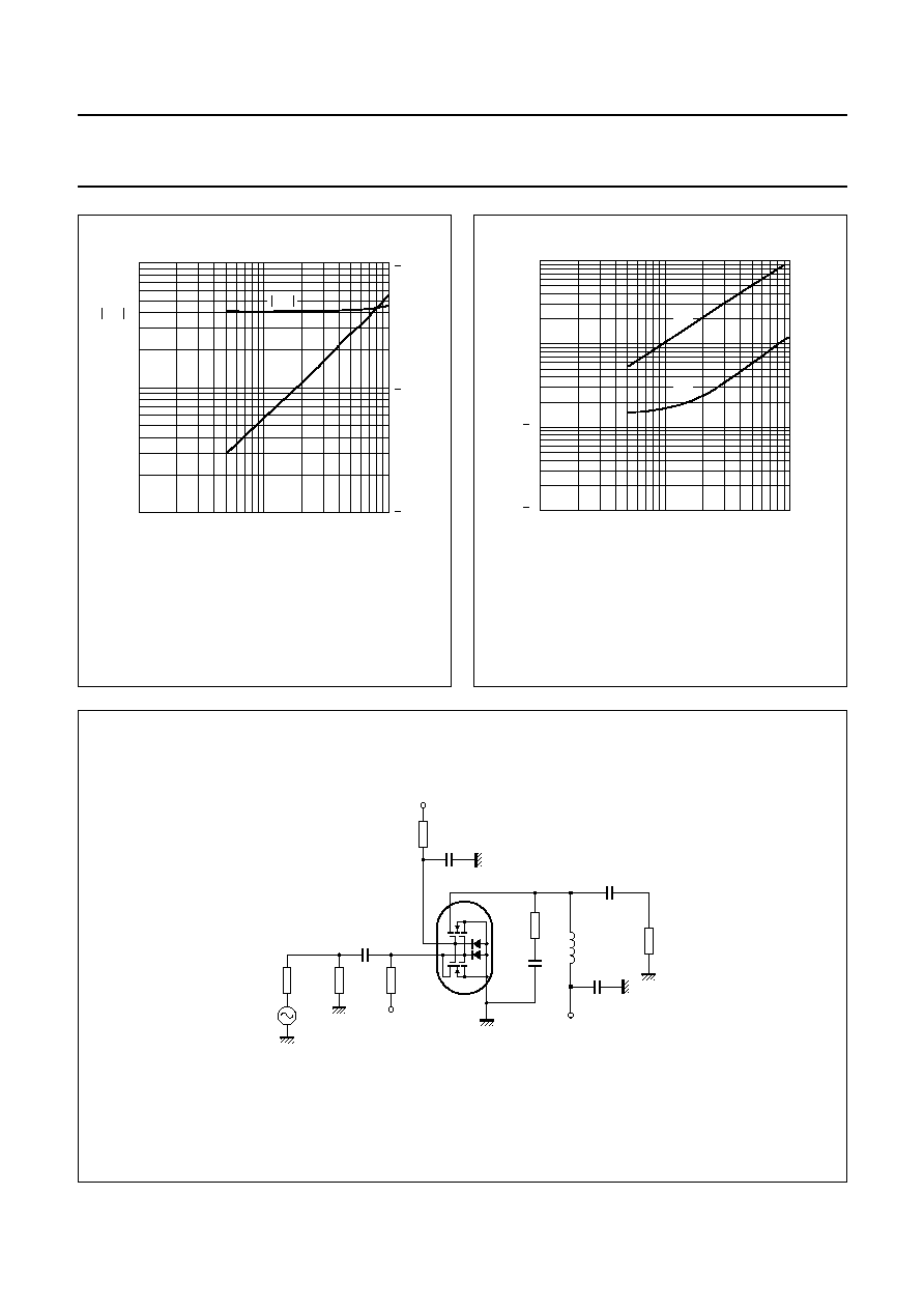
Fig.18 Cross-modulation test set-up.
DUT
VAGC
C1
4.7 nF
R1
10 k
C5
MLD151
C4
4.7 nF
VDS
L1
350 nH
C3
12 pF
2.2
pF
R L
50
50
50
R3
10
VGG
RGEN
V I
R2
4.7 nF
C2
R G1

1995 Apr 25
9
Philips Semiconductors
Product specification
N-channel dual gate MOS-FETs
BF909; BF909R
Table 1
Scattering parameters: T
amb
= 25
∞
C; V
DS
= 5 V; V
G2-S
= 4 V; I
D
= 15 mA
Table 2
Noise data: T
amb
= 25
∞
C; V
DS
= 5 V; V
G2-S
= 4 V; I
D
= 15 mA
f
(MHz)
s
11
s
21
s
12
s
22
MAGNITUDE
(ratio)
ANGLE
(deg)
MAGNITUDE
(ratio)
ANGLE
(deg)
MAGNITUDE
(ratio)
ANGLE
(deg)
MAGNITUDE
(ratio)
ANGLE
(deg)
50
0.985
-
6.4
4.064
172.3
0.001
86.9
0.985
-
3.2
100
0.978
-
12.6
3.997
164.9
0.002
82.7
0.982
-
6.4
200
0.957
-
25.0
3.886
150.8
0.005
74.3
0.973
-
12.6
300
0.931
-
36.5
3.682
137.3
0.006
68.9
0.960
-
18.6
400
0.899
-
47.6
3.484
123.8
0.007
59.6
0.947
-
24.2
500
0.868
-
57.4
3.260
111.7
0.007
57.9
0.936
-
29.6
600
0.848
-
66.6
3.053
101.0
0.006
58.5
0.927
-
34.8
700
0.816
-
74.6
2.829
90.3
0.005
65.5
0.919
-
39.8
800
0.792
-
82.2
2.652
79.9
0.005
83.3
0.913
-
44.6
900
0.772
-
89.3
2.470
69.5
0.005
114.9
0.910
-
49.5
1000
0.754
-
95.6
2.328
59.5
0.006
138.7
0.909
-
54.6
f
(MHz)
F
min
(dB)
opt
r
n
(ratio)
(deg)
800
2.00
0.603
67.71
0.581

1995 Apr 25
10
Philips Semiconductors
Product specification
N-channel dual gate MOS-FETs
BF909; BF909R
PACKAGE OUTLINES
Fig.19 SOT143.
Dimensions in mm.
handbook, full pagewidth
MBC845
10
max
o
10
max
o
30
max
o
1.1
max
0.75
0.60
0.150
0.090
0.1
max
4
3
2
M
0.1
A B
0
0.1
0.48
TOP VIEW
1.4
1.2
2.5
max
3.0
2.8
M
0.2
A B
A
B
1.9
1
0
0.1
0.88
1.7
Fig.20 SOT143R.
Dimensions in mm.
handbook, full pagewidth
MBC844
10
max
o
10
max
o
30
max
o
1.1
max
0.40
0.25
0.150
0.090
0.1
max
3
4
2
1.4
1.2
2.5
max
3.0
2.8
A
B
1.9
M
0.2
A
1
M
0.1
B
TOP VIEW
0.48
0.38
0.88
0.78
1.7

1995 Apr 25
11
Philips Semiconductors
Product specification
N-channel dual gate MOS-FETs
BF909; BF909R
DEFINITIONS
LIFE SUPPORT APPLICATIONS
These products are not designed for use in life support appliances, devices, or systems where malfunction of these
products can reasonably be expected to result in personal injury. Philips customers using or selling these products for
use in such applications do so at their own risk and agree to fully indemnify Philips for any damages resulting from such
improper use or sale.
Data Sheet Status
Objective specification
This data sheet contains target or goal specifications for product development.
Preliminary specification
This data sheet contains preliminary data; supplementary data may be published later.
Product specification
This data sheet contains final product specifications.
Limiting values
Limiting values given are in accordance with the Absolute Maximum Rating System (IEC 134). Stress above one or
more of the limiting values may cause permanent damage to the device. These are stress ratings only and operation
of the device at these or at any other conditions above those given in the Characteristics sections of the specification
is not implied. Exposure to limiting values for extended periods may affect device reliability.
Application information
Where application information is given, it is advisory and does not form part of the specification.