 | –≠–ª–µ–∫—Ç—Ä–æ–Ω–Ω—ã–π –∫–æ–º–ø–æ–Ω–µ–Ω—Ç: BFG540/X | –°–∫–∞—á–∞—Ç—å:  PDF PDF  ZIP ZIP |
Document Outline
- FEATURES
- DESCRIPTION
- PINNING
- QUICK REFERENCE DATA
- LIMITING VALUES
- THERMAL CHARACTERISTICS
- CHARACTERISTICS
- PACKAGE OUTLINES
- DATA SHEET STATUS
- DEFINITIONS
- DISCLAIMERS

DATA SHEET
Product specification
Supersedes data of 1997 Dec 03
2000 May 23
DISCRETE SEMICONDUCTORS
BFG540; BFG540/X; BFG540/XR
NPN 9 GHz wideband transistor

2000 May 23
2
Philips Semiconductors
Product specification
NPN 9 GHz wideband transistor
BFG540; BFG540/X;
BFG540/XR
FEATURES
∑
High power gain
∑
Low noise figure
∑
High transition frequency
∑
Gold metallization ensures
excellent reliability.
DESCRIPTION
NPN silicon planar epitaxial
transistors, intended for wideband
applications in the GHz range, such
as analog and digital cellular
telephones, cordless telephones
(CT1, CT2, DECT, etc.), radar
detectors, satellite TV tuners (SATV),
MATV/CATV amplifiers and repeater
amplifiers in fibre-optical systems.
The transistors are mounted in plastic
SOT143B and SOT143R packages.
PINNING
PIN
DESCRIPTION
BFG540 (Fig.1) Code: N37
1
collector
2
base
3
emitter
4
emitter
BFG540/X (Fig.1) Code: N43
1
collector
2
emitter
3
base
4
emitter
BFG540/XR (Fig.2) Code: N49
1
collector
2
emitter
3
base
4
emitter
Fig.1 SOT143B.
handbook, 2 columns
Top view
MSB014
1
2
3
4
Fig.2 SOT143R.
handbook, 2 columns
Top view
MSB035
1
2
4
3
2000 May 23
3
Philips Semiconductors
Product specification
NPN 9 GHz wideband transistor
BFG540; BFG540/X;
BFG540/XR
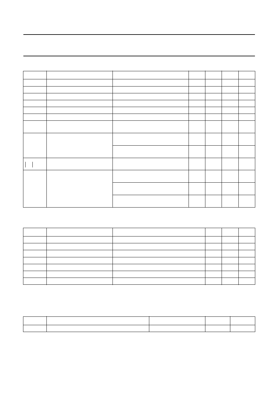
QUICK REFERENCE DATA
LIMITING VALUES
In accordance with the Absolute Maximum System (IEC 60134).
Note
1. T
s
is the temperature at the soldering point of the collector pin.
THERMAL CHARACTERISTICS
Note
1. T
s
is the temperature at the soldering point of the collector pin.
SYMBOL
PARAMETER
CONDITIONS
MIN.
TYP.
MAX.
UNIT
V
CBO
collector-base voltage
open emitter
-
-
20
V
V
CES
collector-emitter voltage
R
BE
= 0
-
-
15
V
I
C
DC collector current
-
-
120
mA
P
tot
total power dissipation
T
s
60
∞
C; note 1
-
-
400
mW
h
FE
DC current gain
I
C
= 40 mA; V
CE
= 8 V; T
j
= 25
∞
C
100
120
250
C
re
feedback capacitance
I
C
= 0; V
CE
= 8 V; f = 1 MHz
-
0.5
-
pF
f
T
transition frequency
I
C
= 40 mA; V
CE
= 8 V; f = 1 GHz;
T
amb
= 25
∞
C
-
9
-
GHz
G
UM
maximum unilateral power gain
I
C
= 40 mA; V
CE
= 8 V; f = 900 MHz;
T
amb
= 25
∞
C
-
18
-
dB
I
C
= 40 mA; V
CE
= 8 V; f = 2 GHz;
T
amb
= 25
∞
C
-
11
-
dB
insertion power gain
I
C
= 40 mA; V
CE
= 8 V; f = 900 MHz;
T
amb
= 25
∞
C
15
16
-
dB
F
noise figure
s
=
opt
; I
C
= 10 mA; V
CE
= 8 V;
f = 900 MHz; T
amb
= 25
∞
C
-
1.3
1.8
dB
s
=
opt
; I
C
= 40 mA; V
CE
= 8 V;
f = 900 MHz; T
amb
= 25
∞
C
-
1.9
2.4
dB
s
=
opt
; I
C
= 10 mA; V
CE
= 8 V;
f = 2 GHz; T
amb
= 25
∞
C
-
2.1
-
dB
SYMBOL
PARAMETER
CONDITIONS
MIN.
MAX.
UNIT
V
CBO
collector-base voltage
open emitter
-
20
V
V
CES
collector-emitter voltage
R
BE
= 0
-
15
V
V
EBO
emitter-base voltage
open collector
-
2.5
V
I
C
DC collector current
-
120
mA
P
tot
total power dissipation
T
s
60
∞
C; note 1
-
400
mW
T
stg
storage temperature
-
65
+150
∞
C
T
j
junction temperature
-
150
∞
C
SYMBOL
PARAMETER
CONDITIONS
VALUE
UNIT
R
th j-s
thermal resistance from junction to soldering point
T
s
60
∞
C; note 1
290
K/W
s
21
2

2000 May 23
4
Philips Semiconductors
Product specification
NPN 9 GHz wideband transistor
BFG540; BFG540/X;
BFG540/XR
CHARACTERISTICS
T
j
= 25
∞
C unless otherwise specified.
Notes
1. G
UM
is the maximum unilateral power gain, assuming s
12
is zero and
2. V
CE
= 8 V; I
C
= 40 mA; R
L
= 50
; T
amb
= 25
∞
C;
f
p
= 900 MHz; f
q
= 902 MHz;
measured at f
(2p
-
q)
= 898 MHz and f
(2q
-
p)
= 904 MHz.
3. d
im
=
-
60 dB (DIN 45004B); I
C
= 40 mA; V
CE
= 8 V; Z
L
= Z
S
= 75
; T
amb
= 25
∞
C;
V
p
= V
O
; V
q
= V
O
-
6 dB; V
r
= V
O
-
6 dB;
f
p
= 795.25 MHz; f
q
= 803.25 MHz; f
r
= 805.25 MHz;
measured at f
(p + q
-
r)
= 793.25 MHz.
4. I
C
= 40 mA; V
CE
= 8 V; V
O
= 275 mV; T
amb
= 25
∞
C;
f
p
= 250 MHz; f
q
= 560 MHz; measured at f
(p + q)
= 810 MHz.
SYMBOL
PARAMETER
CONDITIONS
MIN.
TYP.
MAX.
UNIT
I
CBO
collector cut-off current
I
E
= 0; V
CB
= 8 V
-
-
50
nA
h
FE
DC current gain
I
C
= 40 mA; V
CE
= 8 V
60
120
250
C
e
emitter capacitance
I
C
= i
c
= 0; V
EB
= 0.5 V; f = 1 MHz
-
2
-
pF
C
c
collector capacitance
I
E
= i
e
= 0; V
CB
= 8 V; f = 1 MHz
-
0.9
-
pF
C
re
feedback capacitance
I
C
= 0; V
CB
= 8 V; f = 1 MHz
-
0.5
-
pF
f
T
transition frequency
I
C
= 40 mA; V
CE
= 8 V; f = 1 GHz;
T
amb
= 25
∞
C
-
9
-
GHz
G
UM
maximum unilateral power gain
(note 1)
I
C
= 40 mA; V
CE
= 8 V; f = 900 MHz;
T
amb
= 25
∞
C
-
18
-
dB
I
C
= 40 mA; V
CE
= 8 V; f = 2 GHz;
T
amb
= 25
∞
C
-
11
-
dB
insertion power gain
I
C
= 40 mA; V
CE
= 8 V; f = 900 MHz;
T
amb
= 25
∞
C
15
16
-
dB
F
noise figure
s
=
opt
; I
C
= 10 mA; V
CE
= 8 V;
f = 900 MHz; T
amb
= 25
∞
C
-
1.3
1.8
dB
s
=
opt
; I
C
= 40 mA; V
CE
= 8 V;
f = 900 MHz; T
amb
= 25
∞
C
-
1.9
2.4
dB
s
=
opt
; I
C
= 10 mA; V
CE
= 8 V;
f = 2 GHz; T
amb
= 25
∞
C
-
2.1
-
dB
P
L1
output power at 1 dB gain
compression
I
C
= 40 mA; V
CE
= 8 V; R
L
= 50
;
f = 900 MHz; T
amb
= 25
∞
C
-
21
-
dBm
ITO
third order intercept point
note 2
-
34
-
dBm
V
O
output voltage
note 3
-
500
-
mV
d
2
second order intermodulation
distortion
note 4
-
-
50
-
dB
s
21
2
G
UM
10
s
21
2
1
s
11
2
≠
(
)
1
s
22
2
≠
(
)
-------------------------------------------------------- dB.
log
=

2000 May 23
5
Philips Semiconductors
Product specification
NPN 9 GHz wideband transistor
BFG540; BFG540/X;
BFG540/XR
Fig.3 Power derating curve.
handbook, halfpage
0
50
100
200
600
200
0
400
MBG249
150
P
tot
(mW)
T
s
(
o
C)
V
CE
10 V.
Fig.4
DC current gain as a function of collector
current.
V
CE
= 8 V; T
j
= 25
∞
C.
handbook, halfpage
0
250
50
100
150
200
MRA749
10
-
2
10
-
1
1
10
10
2
hFE
IC (mA)
Fig.5
Feedback capacitance as a function of
collector-base voltage.
I
C
= 0; f = 1 MHz.
handbook, halfpage
0
4
Cre
(pF)
VCB (V)
8
12
1
0
0.8
0.6
0.4
0.2
MRA750
Fig.6
Transition frequency as a function of
collector current.
f = 1 GHz; T
amb
= 25
∞
C.
handbook, halfpage
12
0
4
8
fT
(GHz)
IC (mA)
MRA751
10
-
1
1
10
10
2
VCE = 8 V
VCE = 4 V