 | –≠–ª–µ–∫—Ç—Ä–æ–Ω–Ω—ã–π –∫–æ–º–ø–æ–Ω–µ–Ω—Ç: BFG67W/X | –°–∫–∞—á–∞—Ç—å:  PDF PDF  ZIP ZIP |
Document Outline
- FEATURES
- APPLICATIONS
- DESCRIPTION
- MARKING
- PINNING
- QUICK REFERENCE DATA
- LIMITING VALUES
- THERMAL CHARACTERISTICS
- CHARACTERISTICS
- SPICE parameters for the BFG67W crystal
- List of components
- PACKAGE OUTLINES
- DEFINITIONS
- LIFE SUPPORT APPLICATIONS

DATA SHEET
Product specification
File under Discrete Semiconductors, SC14
August 1995
DISCRETE SEMICONDUCTORS
Philips Semiconductors
BFG67W
BFG67W/X; BFG67W/XR
NPN 8 GHz wideband transistor

August 1995
2
Philips Semiconductors
Product specification
NPN 8 GHz wideband transistor
BFG67W
BFG67W/X; BFG67W/XR
FEATURES
∑
High power gain
∑
Low noise figure
∑
Gold metallization ensures
excellent reliability.
APPLICATIONS
They are intended for wideband
applications in the GHz range such as
analog satellite television systems
and portable RF communication
equipment.
DESCRIPTION
NPN silicon planar epitaxial
transistors in plastic, 4-pin
dual-emitter SOT343 and SOT343R
packages.
MARKING
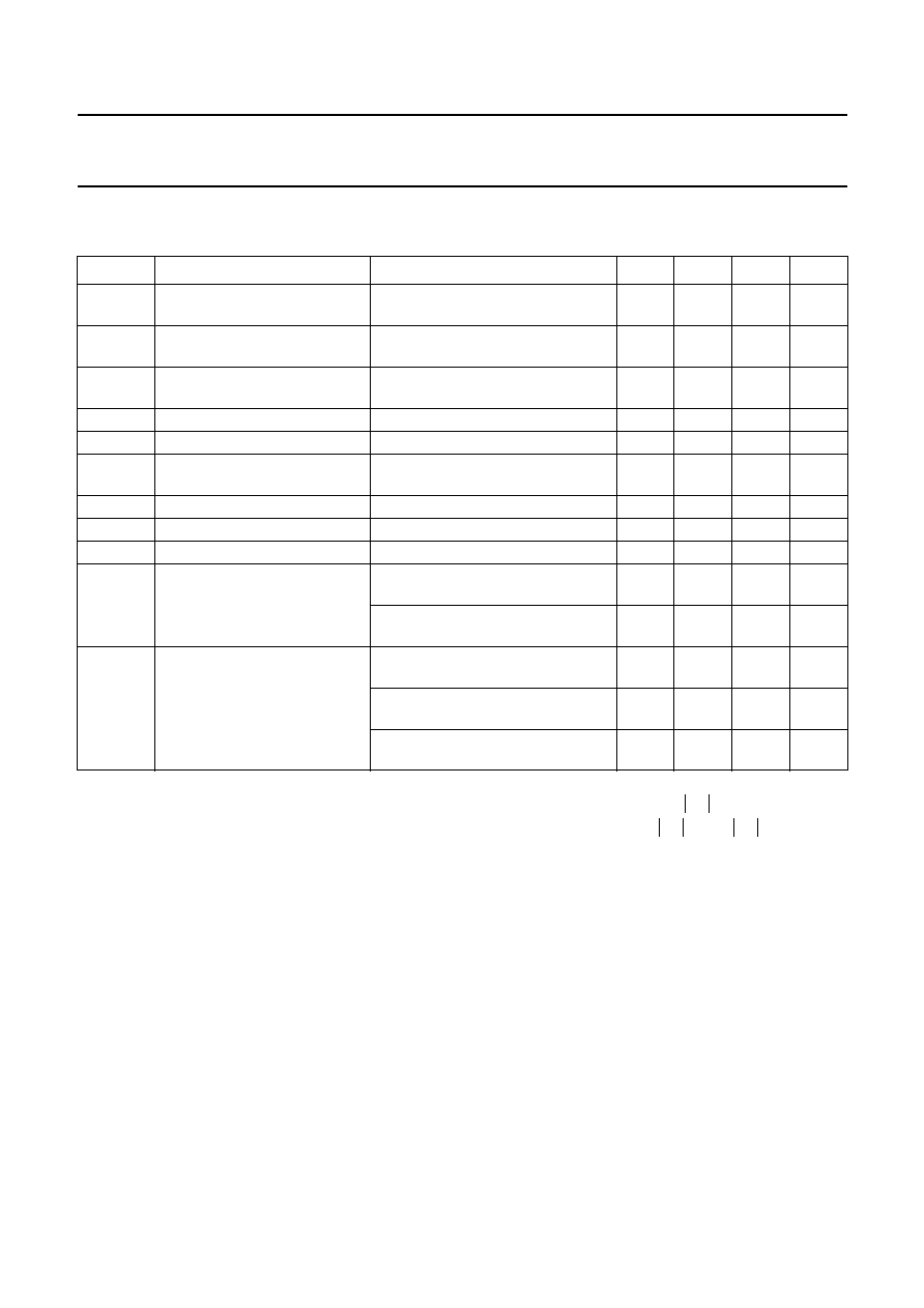
PINNING
TYPE NUMBER
CODE
BFG67W
V2
BFG67W/X
V6
BFG67W/XR
V7
PIN
DESCRIPTION
BFG67W (see Fig.1)
1
collector
2
base
3
emitter
4
emitter
BFG67W/X (see Fig.1)
1
collector
2
emitter
3
base
4
emitter
BFG67W/XR (see Fig.2)
1
collector
2
emitter
3
base
4
emitter
Fig.1 SOT343.
fpage
Top view
MBK523
2
1
3
4
Fig.2 SOT343R.
alfpage
Top view
MSB842
2
1
4
3
QUICK REFERENCE DATA
SYMBOL
PARAMETER
CONDITIONS
MIN. TYP. MAX. UNIT
V
CBO
collector-base voltage
open emitter
-
-
20
V
V
CEO
collector-emitter voltage
open base
-
-
10
V
I
C
collector current (DC)
-
-
50
mA
P
tot
total power dissipation
up to T
s
= 85
∞
C
-
-
500
mW
h
FE
DC current gain
I
C
= 15 mA; V
CE
= 5 V
60
100
-
C
re
feedback capacitance
I
C
= 0; V
CE
= 8 V; f = 1 MHz
-
0.5
-
pF
f
T
transition frequency
I
C
= 15 mA; V
CE
= 8 V; f = 500 MHz; T
amb
= 25
∞
C
-
7.5
-
GHz
G
UM
maximum unilateral
power gain
I
C
= 15 mA; V
CE
= 8 V; f = 1 GHz; T
amb
= 25
∞
C
-
15.5
-
dB
F
noise figure
s
=
opt
; I
C
= 5 mA; V
CE
= 8 V; f = 2 GHz
-
2.2
-
dB

August 1995
3
Philips Semiconductors
Product specification
NPN 8 GHz wideband transistor
BFG67W
BFG67W/X; BFG67W/XR
LIMITING VALUES
In accordance with the Absolute Maximum Rating System (IEC 134).
SYMBOL
PARAMETER
CONDITIONS
MIN.
MAX.
UNIT
V
CBO
collector-base voltage
open emitter
-
20
V
V
CEO
collector-emitter voltage
open base
-
10
V
V
EBO
emitter-base voltage
open collector
-
2.5
V
I
C
collector current (DC)
-
50
mA
P
tot
total power dissipation
up to T
s
= 85
∞
C; see Fig.3; note 1
-
500
mW
T
stg
storage temperature
-
65
+150
∞
C
T
j
junction temperature
-
175
∞
C
Fig.3 Power derating curve.
handbook, halfpage
0
50
100
200
400
0
MBG248
150
T ( C)
o
s
Ptot
(mW)
600
200
THERMAL CHARACTERISTICS
Note to the "Limiting values" and "Thermal characteristics"
1. T
s
is the temperature at the soldering point of the collector pin.
SYMBOL
PARAMETER
CONDITIONS
VALUE
UNIT
R
th j-s
thermal resistance from junction to soldering point
up to T
s
= 85
∞
C; note 1
180
K/W
August 1995
4
Philips Semiconductors
Product specification
NPN 8 GHz wideband transistor
BFG67W
BFG67W/X; BFG67W/XR
CHARACTERISTICS
T
j
= 25
∞
C (unless otherwise specified).
Note
1. G
UM
is the maximum unilateral power gain, assuming s
12
is zero.
SYMBOL
PARAMETER
CONDITIONS
MIN.
TYP.
MAX.
UNIT
V
(BR)CBO
collector-base breakdown
voltage
open emitter; I
C
= 10
µ
A; I
E
= 0
-
-
20
V
V
(BR)CEO
collector-emitter breakdown
voltage
open base; I
C
= 10 mA; I
B
= 0
-
-
10
V
V
(BR)EBO
emitter-base breakdown
voltage
open collector; I
E
= 10
µ
A; I
C
= 0
-
-
2.5
V
I
CBO
collector cut-off current
open emitter; V
CB
= 5 V; I
E
= 0
-
-
50
nA
h
FE
DC current gain
I
C
= 15 mA; V
CE
= 5 V
60
100
-
f
T
transition frequency
I
C
= 15 mA; V
CE
= 8 V; f = 500 MHz;
T
amb
= 25
∞
C
-
7.5
-
GHz
C
c
collector capacitance
I
E
= i
e
= 0; V
CE
= 8 V; f = 1 MHz
-
0.7
-
pF
C
e
emitter capacitance
I
C
= i
c
= 0; V
EB
= 0.5 V; f = 1 MHz
-
1.3
-
pF
C
re
feedback capacitance
I
C
= 0; V
CE
= 8 V; f = 1 MHz
-
0.5
-
pF
G
UM
maximum unilateral power
gain; note 1
I
C
= 15 mA; V
CE
= 8 V; f = 1 GHz;
T
amb
= 25
∞
C
-
15.5
-
dB
I
C
= 15 mA; V
CE
= 8 V; f = 2 GHz;
T
amb
= 25
∞
C
-
10
-
dB
F
noise figure
s
=
opt
; I
C
= 5 mA; V
CE
= 8 V;
f = 1 GHz
-
1.3
-
dB
s
=
opt
; I
C
= 15 mA; V
CE
= 8 V;
f = 1 GHz
-
1.7
-
dB
s
=
opt
; I
C
= 5 mA; V
CE
= 8 V;
f = 2 GHz
-
2.2
-
dB
G
UM
10
s
21
2
1
s
11
2
≠
(
)
1
s
22
2
≠
(
)
------------------------------------------------------------ dB.
log
=

August 1995
5
Philips Semiconductors
Product specification
NPN 8 GHz wideband transistor
BFG67W
BFG67W/X; BFG67W/XR
V
CE
= 5 V.
Fig.4
DC current gain as a function of collector
current; typical values.
handbook, halfpage
0
120
80
40
0
20
40
MBB301
60
I (mA)
C
FE
h
I
C
= 0; f = 1 MHz.
Fig.5
Feedback capacitance as a function of
collector-base voltage; typical values.
handbook, halfpage
0
4
8
16
1
0
0.8
MLB984
12
0.6
0.4
0.2
C re
(pF)
V CB (V)
Fig.6
Transition frequency as a function of
collector current; typical values.
f = 2 GHz; V
CE
= 8 V; T
amb
= 25
∞
C.
handbook, halfpage
0
10
20
40
10
8
4
0
6
MLB985
30
I (mA)
C
(GHz)
T
f
2