 | ÐлекÑÑоннÑй компоненÑ: BFR505 | СкаÑаÑÑ:  PDF PDF  ZIP ZIP |
Äîêóìåíòàöèÿ è îïèñàíèÿ www.docs.chipfind.ru

DATA SHEET
Product specification
File under Discrete Semiconductors, SC14
September 1995
DISCRETE SEMICONDUCTORS
BFR505
NPN 9 GHz wideband transistor
September 1995
2
Philips Semiconductors
Product specification
NPN 9 GHz wideband transistor
BFR505
FEATURES
·
High power gain
·
Low noise figure
·
High transition frequency
·
Gold metallization ensures
excellent reliability.
DESCRIPTION
The BFR505 is an npn silicon planar
epitaxial transistor, intended for
applications in the RF frontend in
wideband applications in the GHz
range, such as analog and digital
cellular telephones, cordless
telephones (CT1, CT2, DECT, etc.),
radar detectors, pagers and satellite
TV tuners (SATV).
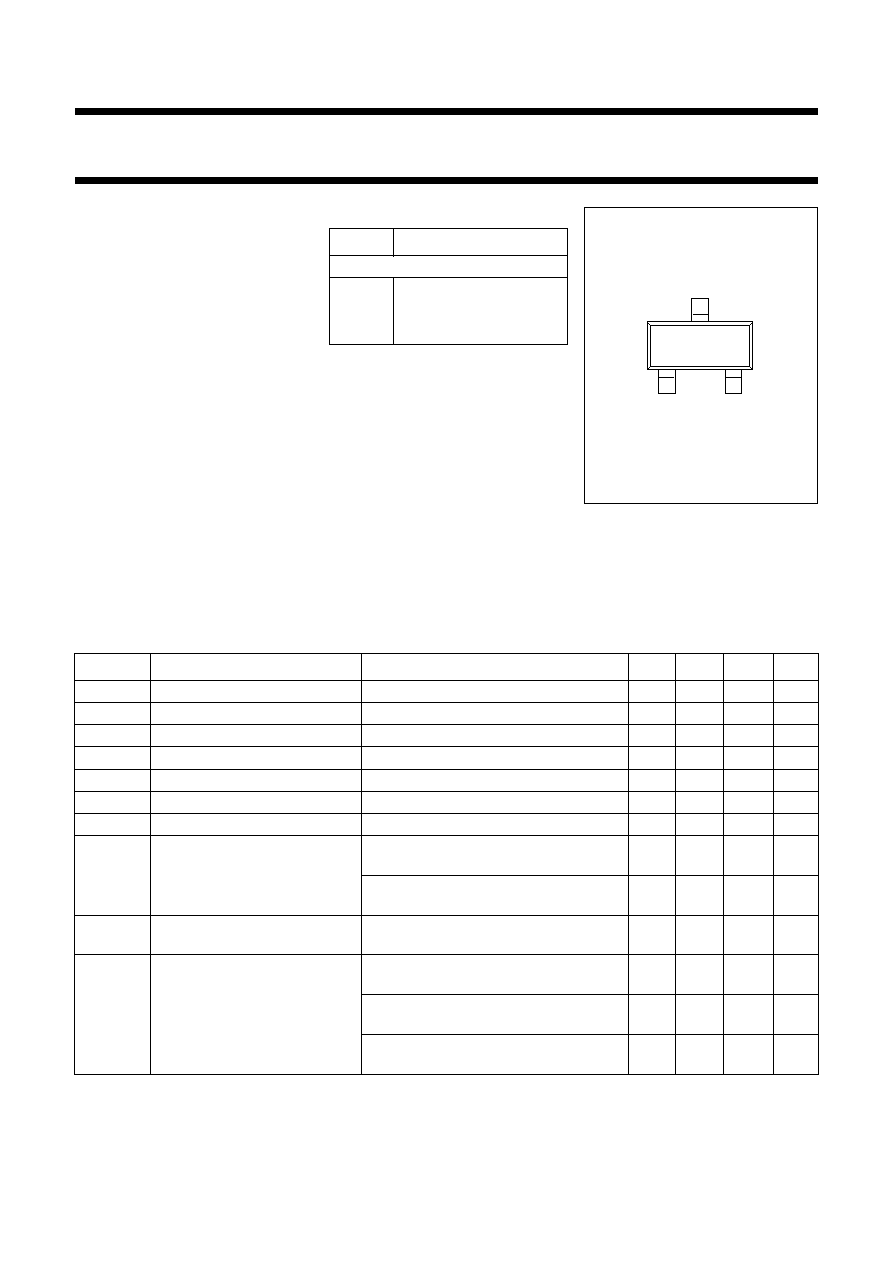
The transistor is encapsulated in a
plastic SOT23 envelope.
PINNING
PIN
DESCRIPTION
Code: N30
1
base
2
emitter
3
collector
Fig.1 SOT23.
fpage
MSB003
Top view
1
2
3
QUICK REFERENCE DATA
Note
1. T
s
is the temperature at the soldering point of the collector tab.
SYMBOL
PARAMETER
CONDITIONS
MIN.
TYP.
MAX.
UNIT
V
CBO
collector-base voltage
open emitter
-
-
20
V
V
CES
collector-emitter voltage
R
BE
= 0
-
-
15
V
I
C
DC collector current
-
-
18
mA
P
tot
total power dissipation
up to T
s
= 135
°
C; note 1
-
-
150
mW
h
FE
DC current gain
I
C
= 5 mA; V
CE
= 6 V
60
120
250
C
re
feedback capacitance
I
C
= i
c
= 0; V
CB
= 6 V; f = 1 MHz
-
0.3
-
pF
f
T
transition frequency
I
C
= 5 mA; V
CE
= 6 V; f = 1 GHz
-
9
-
GHz
G
UM
maximum unilateral
power gain
I
C
= 5 mA; V
CE
= 6 V;
T
amb
= 25
°
C; f = 900 MHz
-
17
-
dB
I
C
= 5 mA; V
CE
= 6 V;
T
amb
= 25
°
C; f = 2 GHz
-
10
-
dB
S
21
2
insertion power gain
I
C
= 5 mA; V
CE
= 6 V;
T
amb
= 25
°
C; f = 900 MHz
13
14
-
dB
F
noise figure
s
=
opt
; I
C
= 1.25 mA; V
CE
= 6 V;
T
amb
= 25
°
C; f = 900 MHz
-
1.2
1.7
dB
s
=
opt
; I
C
= 5 mA; V
CE
= 6 V;
T
amb
= 25
°
C; f = 900 MHz
-
1.6
2.1
dB
s
=
opt
; I
C
= 1.25 mA; V
CE
= 6 V;
T
amb
= 25
°
C; f = 2 GHz
-
1.9
-
dB

September 1995
3
Philips Semiconductors
Product specification
NPN 9 GHz wideband transistor
BFR505
LIMITING VALUES
In accordance with the Absolute Maximum System (IEC 134).
THERMAL RESISTANCE
Note
1. T
s
is the temperature at the soldering point of the collector tab.
SYMBOL
PARAMETER
CONDITIONS
MIN.
MAX.
UNIT
V
CBO
collector-base voltage
open emitter
-
20
V
V
CES
collector-emitter voltage
R
BE
= 0
-
15
V
V
EBO
emitter-base voltage
-
2.5
V
I
C
DC collector current
continuous
-
18
mA
P
tot
total power dissipation
up to T
s
= 135
°
C; note 1
-
150
mW
T
stg
storage temperature
-
65
150
°
C
T
j
junction temperature
-
175
°
C
SYMBOL
PARAMETER
THERMAL RESISTANCE
R
th j-s
from junction to soldering point (note 1)
260 K/W

September 1995
4
Philips Semiconductors
Product specification
NPN 9 GHz wideband transistor
BFR505
CHARACTERISTICS
T
j
= 25
°
C unless otherwise specified.
Notes
1. G
UM
is the maximum unilateral power gain, assuming S
12
is zero and
2. I
C
= 5 mA; V
CE
= 6 V; R
L
= 50
; T
amb
= 25
°
C;
f
p
= 900 MHz; f
q
= 902 MHz;
measured at f
(2p
-
q)
= 898 MHz and f
(2q
-
p)
= 904 MHz.
SYMBOL
PARAMETER
CONDITIONS
MIN. TYP. MAX.
UNIT
I
CBO
collector cut-off current
I
E
= 0; V
CB
= 6 V
-
-
50
nA
h
FE
DC current gain
I
C
= 5 mA; V
CE
= 6 V
60
120
250
C
e
emitter capacitance
I
C
= i
c
= 0; V
EB
= 0.5 V; f = 1 MHz
-
0.4
-
pF
C
c
collector capacitance
I
E
= i
e
= 0; V
CB
= 6 V; f = 1 MHz
-
0.4
-
pF
C
re
feedback capacitance
I
C
= 0; V
CB
= 6 V; f = 1 MHz
-
0.3
-
pF
f
T
transition frequency
I
C
= 5 mA; V
CE
= 6 V; f = 1 GHz
-
9
-
GHz
G
UM
maximum unilateral power
gain (note 1)
I
C
= 5 mA; V
CE
= 6 V;
T
amb
= 25
°
C; f = 900 MHz
-
17
-
dB
I
C
= 5 mA; V
CE
= 6 V;
T
amb
= 25
°
C; f = 2 GHz
-
10
-
dB
S
21
2
insertion power gain
I
C
= 5 mA; V
CE
= 6 V;
T
amb
= 25
°
C; f = 900 MHz
13
14
-
dB
F
noise figure
s
=
opt
; I
C
= 5 mA; V
CE
= 6 V;
T
amb
= 25
°
C; f = 900 MHz
-
1.2
1.7
dB
s
=
opt
; I
C
= 5 mA; V
CE
= 6 V;
T
amb
= 25
°
C; f = 900 MHz
-
1.6
2.1
dB
s
=
opt
; I
C
= 5 mA; V
CE
= 6 V;
T
amb
= 25
°
C; f = 2 GHz
-
1.9
-
dB
P
L1
output power at 1 dB gain
compression
I
C
= 5 mA; V
CE
= 6 V; R
L
= 50
;
T
amb
= 25
°
C; f = 900 MHz
-
4
-
dBm
ITO
third order intercept point
note 2
-
10
-
dBm
G
UM
10
S
21
2
1
S
11
2
1
S
22
2
--------------------------------------------------------------
dB.
log
=
September 1995
5
Philips Semiconductors
Product specification
NPN 9 GHz wideband transistor
BFR505
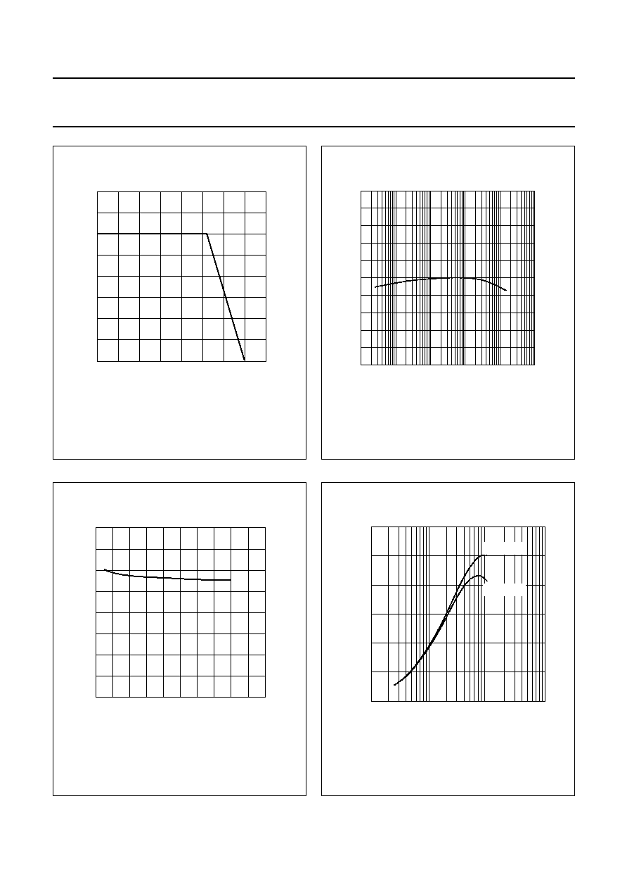
Fig.2 Power derating curve.
handbook, halfpage
0
50
100
200
200
150
50
0
100
MRA718 - 1
150
P
tot
(mW)
T
s
(
o
C)
Fig.3
DC current gain as a function of collector
current.
V
CE
= 6 V.
handbook, halfpage
MRA719
0
250
50
100
150
200
hFE
IC (mA)
10
-
2
10
-
1
10
-
3
1
10
10
2
Fig.4
Feedback capacitance as a function of
collector-base voltage.
I
c
= 0; f = 1 MHz.
handbook, halfpage
0
2
10
0.4
Cre
(pF)
0.3
0.1
0
0.2
4
6
8
VCB (V)
MRA720
Fig.5
Transition frequency as a function of
collector current.
T
amb
= 25
°
C; f = 1 GHz.
MRA721
10
2
10
-
1
10
1
4
8
12
fT
(GHz)
IC (mA)
VCE = 3V
VCE = 6V